Image sensor, semiconductor device and image sensor system

a technology of image sensor and semiconductor device, which is applied in the field of image sensor, semiconductor device for device isolation, and image sensor system, can solve the problems of unavoidable diffusion of impurity ions, deterioration of image realization characteristics of cmos image sensor, and loss of photodiode area, etc., to achieve excellent insulation characteristics and micro device isolation, the effect of minimizing the loss of a photodiode area

Inactive Publication Date: 2014-12-04
SK HYNIX INC
View PDF2 Cites 1 Cited by
  • Summary
  • Abstract
  • Description
  • Claims
  • Application Information

AI Technical Summary

Benefits of technology

[0015]Various exemplary embodiments are directed to an image sensor, where a loss of a photodiode area is minimized while a dark current source is removed, and a method of fabricating the image sensor. Also, various exemplary embodiments are directed to a semiconductor device, which is capable of realizing excellent insulation characteristics and micro device isolation, and a method of fabricating the semiconductor device.

Problems solved by technology

The dark current may deteriorate characteristics of the image sensor in which an optical image is converted into an electric signal.
As a result, an area of the photodiode 11 becomes reduced due to the impurity ions diffused to the photodiode 11, thereby resulting in deterioration in image realization characteristics of the CMOS image sensor.
In detail, diffusion of the impurity ions is unavoidably caused by the annealing process.
As a result, the area of the photodiode 11, which receives light, decreases, and, thus, the image realization characteristics of the CMOS image sensor may deteriorate.

Method used


Image

  • Image sensor, semiconductor device and image sensor system
  • Image sensor, semiconductor device and image sensor system
  • Image sensor, semiconductor device and image sensor system

Examples


Embodiment Construction

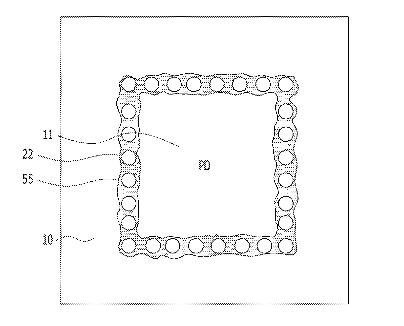
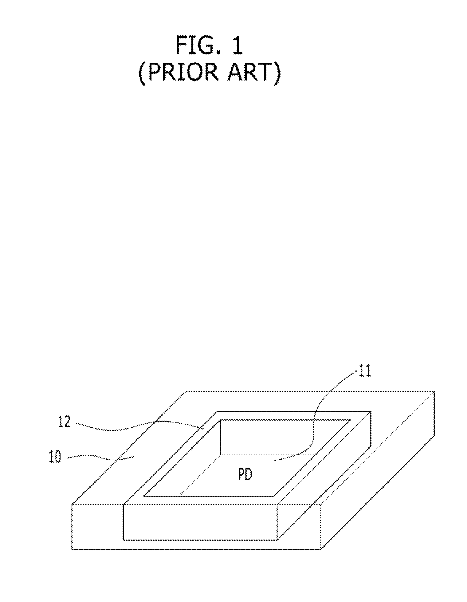
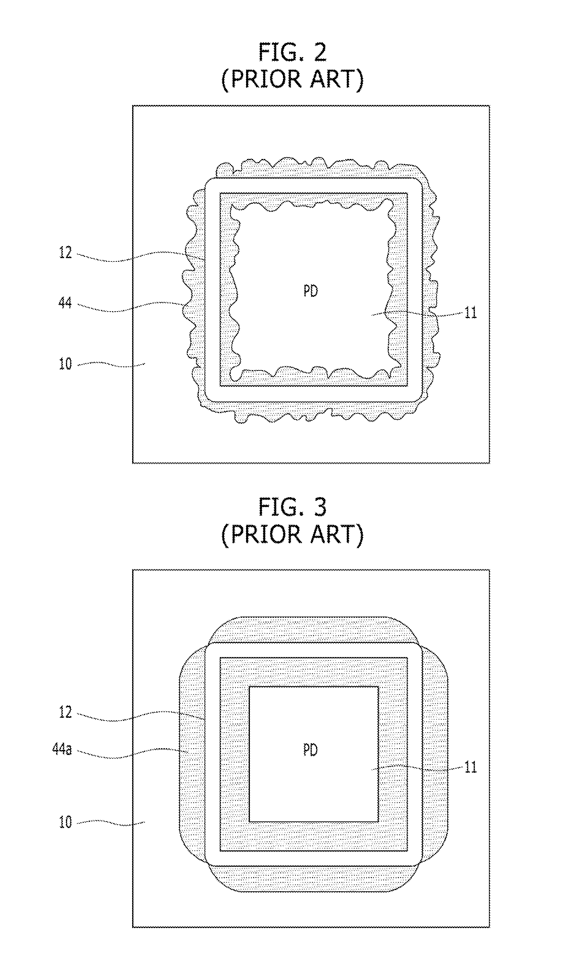
[0028]Various exemplary embodiments will be described below in more detail with reference to the accompanying drawings. The present invention may, however, be embodied in different forms and should not be construed as limited to the embodiments set forth herein. Rather, these embodiments are provided so that this disclosure will be thorough and complete, and will fully convey the scope of the present invention to those skilled in the art. Throughout the disclosure, reference numerals correspond directly to the like numbered parts in the various figures and embodiments of the present invention.

[0029]In the description of embodiments, when layers (or layer), regions, pattern, or structures are referred to as being formed “on or “under” layers (layer), regions, pads or patterns, all of the cases in which the layers (layer), the regions, the pattern, and the structures are formed directly and indirectly “on” or “under” are included.

[0030]Further, a reference for “on” or “under” is refer...


PUM


Abstract

The present technology provides a semiconductor device that includes a substrate including an active region and an device isolation region, a plurality of micro insulation structures formed in the substrate of the device isolation region and spaced from each other, and an impurity region suitable for filling spaces between the micro insulation structures and for surrounding the micro insulation structures in the substrate of the device isolation region, and a method of fabricating the semiconductor device by improving a method of forming device isolation regions that insulate active regions. In particular, discontinuous micro insulation structures are suggested.

Description

CROSS-REFERENCE TO RELATED APPLICATIONS[0001]The present application claims priority of Korean Patent. Application No. 10-2013-0063296, filed on Jun., 03 2013, which is incorporated herein by reference in its entirety.BACKGROUND[0002]1. Field[0003]Exemplary embodiments of the present invention relate to an image sensor, a semiconductor device for device isolation, and an image sensor system.[0004]2. Description of the Related Art[0005]With rapid progress of high speed and high integration of semiconductor devices, demands for miniaturization of patterns and high accuracy of pattern dimensions have increased. The same also applies to device isolation layers occupying a relatively large region as well as patterns formed in active regions.[0006]In most present semiconductor devices, the device isolation layers are formed using a Shallow Trench Isolation (STI) process to ensure the sizes of active regions and realize high-integrated devices.[0007]FIGS. 1 to 3 are diagrams illustrating a...

Claims


Application Information

Patent Timeline
Patent Type & Authority Applications(United States)
IPC IPC(8): H01L27/146H04N5/378
CPCH04N5/378H01L27/1463H01L21/762H01L27/146
Inventor KIM, DO-HYUNGMOON, JANG-WONLIM, YOUN-SUBKIM, DO-HWAN
Owner SK HYNIX INC
Why Eureka
Try Eureka