Light receiving element and optical device
a technology of light receiving element and optical device, which is applied in the direction of semiconductor devices, electrical devices, nanotechnology, etc., can solve the problems of excessive responsivity in the type i wavelength region and in the longer-wavelength region, and achieve the effect of small fluctuations in responsivity
- Summary
- Abstract
- Description
- Claims
- Application Information
AI Technical Summary
Benefits of technology
Problems solved by technology
Method used
Image
Examples
first embodiment
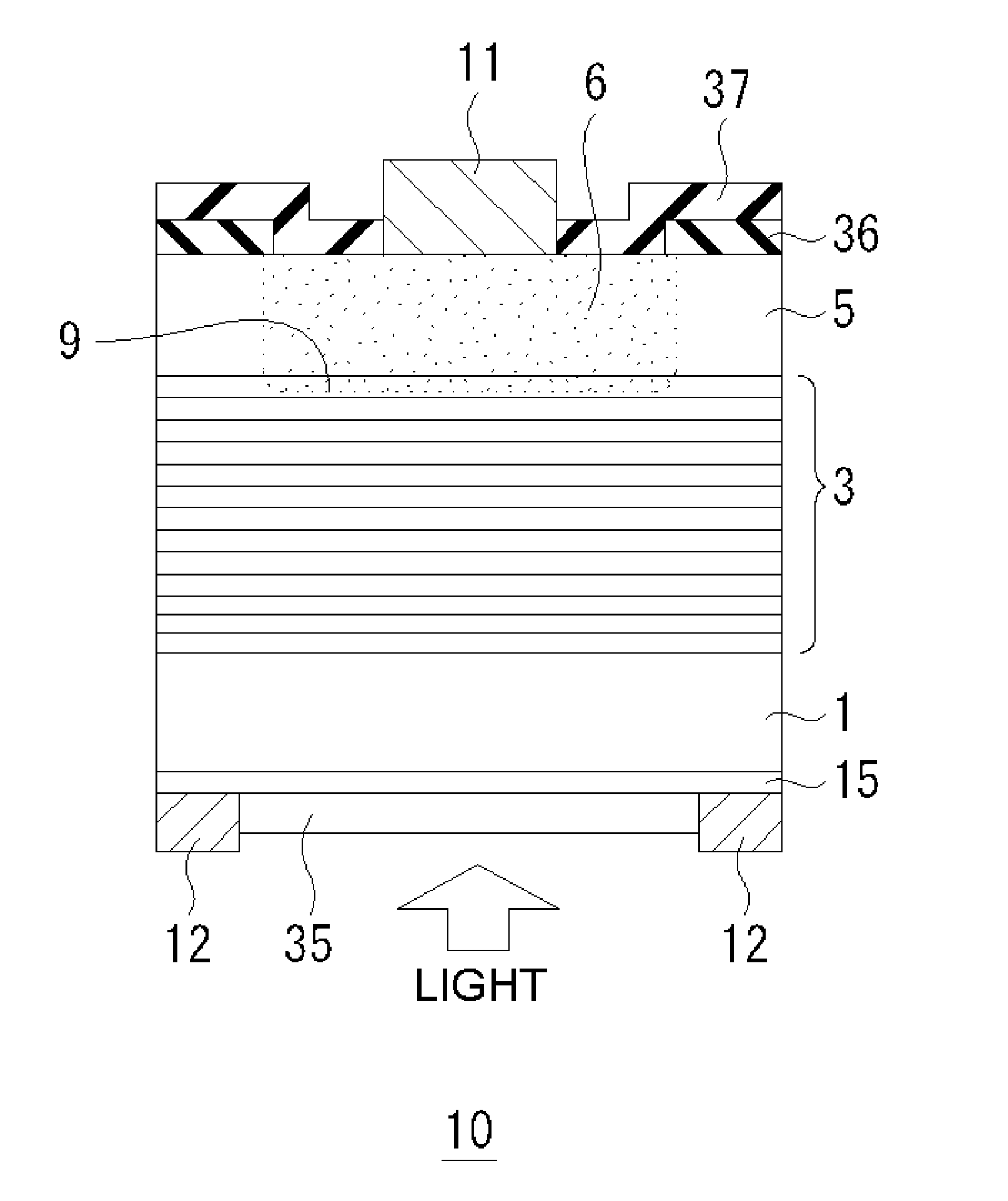
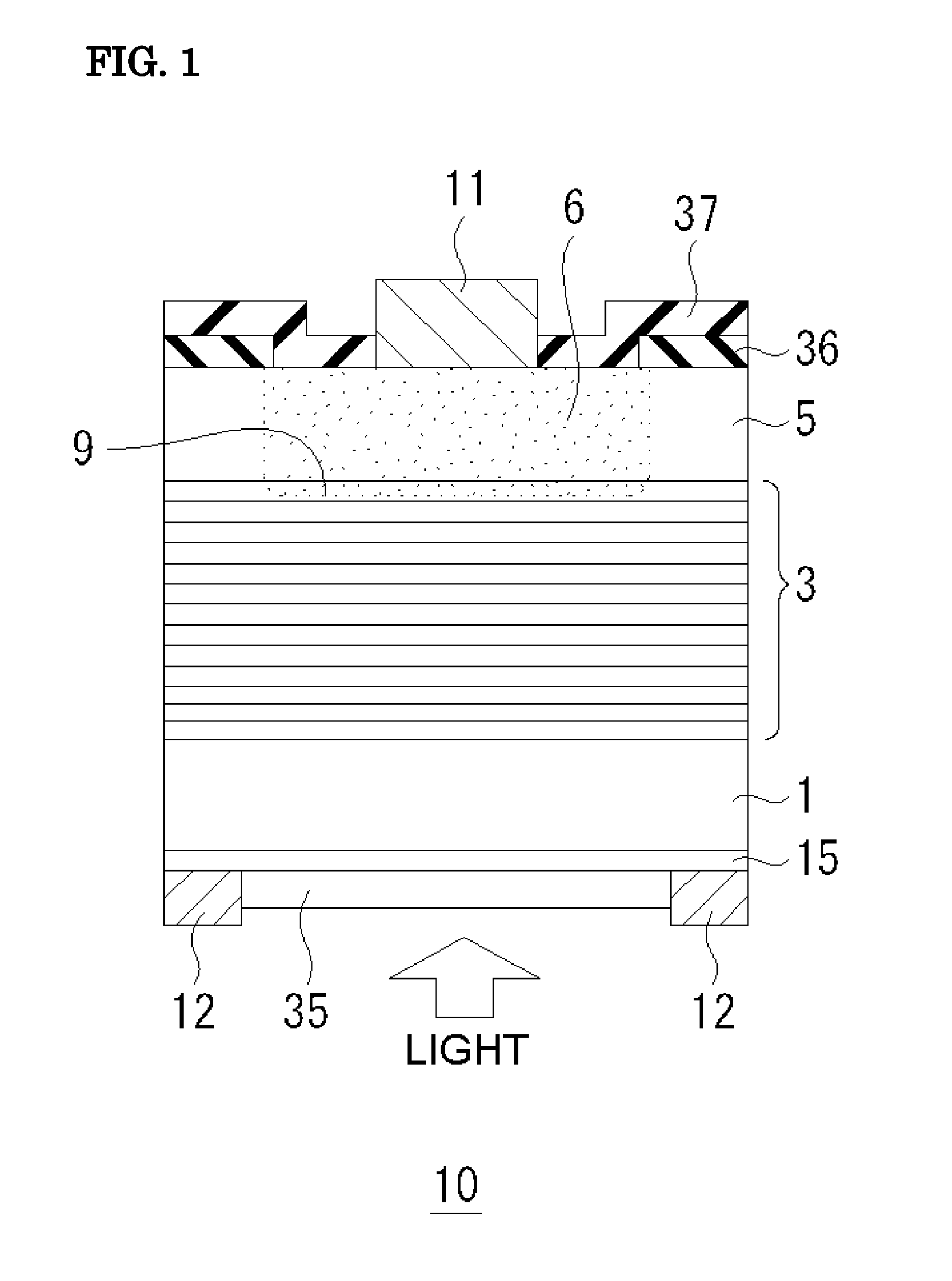
[0068]FIG. 1 is a schematic view of a light-receiving element 10 according to a first embodiment of the present invention. Although FIG. 1 illustrates a single pixel, the single pixel may be or even should be one of one- or two-dimensionally arranged pixels. More specifically, FIG. 1 illustrates a light-receiving element 10 having a single pixel or part of a light-receiving element 10 having one- or two-dimensionally arranged pixels. This applies to all the light-receiving elements according to the subsequent embodiments and will not be further described.
[0069]The following is an epitaxial layered structure of a III-V group compound semiconductor in the light-receiving element 10.
[0070]n-type InGaAs absorption layer 15 / sulfur (S)-doped n-type InP substrate 1 / light-receiving layer 3 having (InGaAs / GaAsSb) type II multi-quantum well structure / InP window layer 5
[0071]The light-receiving layer 3 has a multi-quantum well structure. The term “light-receiving layer 3” and “multi-quantum we...
second embodiment
[0087]FIG. 6 is a schematic view of a light-receiving element 10 according to a second embodiment of the present invention. The light-receiving element 10 has the following layered structure of a III-V group compound semiconductor.
[0088]Sulfur (S)-doped n-type InP substrate 1 / n-type InGaAs absorption layer 15 / n-type hole-extinguishing layer 25 / light-receiving layer 3 having type II (InGaAs / GaAsSb) multi-quantum well structure / InGaAs diffusion concentration distribution control layer 4 / InP window layer 5
[0089]The light-receiving element 10 is different from the light-receiving element according to the first embodiment illustrated in FIG. 1 in the following points.
[0090](1) The InGaAs absorption layer 15 is disposed on the light-receiving layer 3 side of the InP substrate 1.
[0091](2) A hole-extinguishing layer 25 is disposed between the InGaAs absorption layer 15 and the light-receiving layer 3.
[0092](3) An InGaAs diffusion concentration distribution control layer 4 is disposed betwee...
third embodiment
[0097]FIG. 7 is a schematic view of a light-receiving element 10 according to a third embodiment of the present invention. The light-receiving element 10 has the following layered structure of a III-V group compound semiconductor.
[0098]Iron (Fe)-doped semi-insulating InP substrate 1 / n-type InGaAs absorption layer 15 / n-type hole-extinguishing layer 25 / light-receiving layer 3 having type II (InGaAs / GaAsSb) multi-quantum well structure / InGaAs diffusion concentration distribution control layer 4 / InP window layer 5
[0099]Selective diffusion of zinc (Zn) under the top surface of the InP window layer 5 through an opening in a selective diffusion mask pattern 36 forms a p-type region 6 and a p-n junction 9 as defined above in front of the p-type region 6.
[0100]The light-receiving element 10 is different from the light-receiving element according to the second embodiment illustrated in FIG. 6 in the following points.
[0101](1) The InP substrate 1 is an iron (Fe)-doped semi-insulating InP subst...
PUM
 Abstract
Description
Claims
Application Information


