Light receiving element and optical device
- Summary
- Abstract
- Description
- Claims
- Application Information
AI Technical Summary
Benefits of technology
Problems solved by technology
Method used
Image

Examples
first embodiment
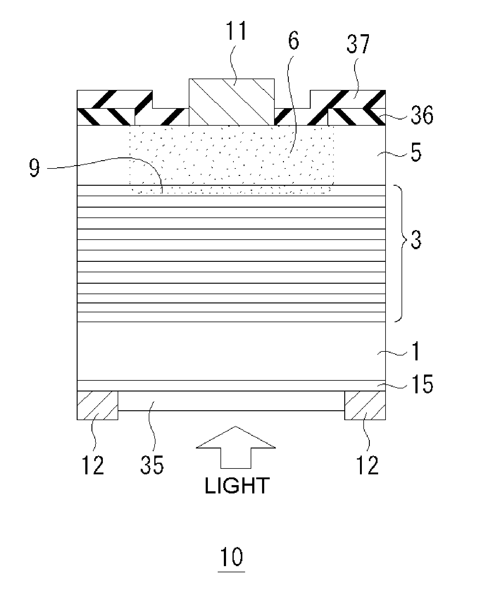
[0068]FIG. 1 is a schematic view of a light-receiving element 10 according to a first embodiment of the present invention. Although FIG. 1 illustrates a single pixel, the single pixel may be or even should be one of one- or two-dimensionally arranged pixels. More specifically, FIG. 1 illustrates a light-receiving element 10 having a single pixel or part of a light-receiving element 10 having one- or two-dimensionally arranged pixels. This applies to all the light-receiving elements according to the subsequent embodiments and will not be further described.
[0069]The following is an epitaxial layered structure of a III-V group compound semiconductor in the light-receiving element 10.
[0070]n-type InGaAs absorption layer 15 / sulfur (S)-doped n-type InP substrate 1 / light-receiving layer 3 having (InGaAs / GaAsSb) type II multi-quantum well structure / InP window layer 5
[0071]The light-receiving layer 3 has a multi-quantum well structure. The term “light-receiving layer 3” and “multi-quantum we...
second embodiment
[0087]FIG. 6 is a schematic view of a light-receiving element 10 according to a second embodiment of the present invention. The light-receiving element 10 has the following layered structure of a III-V group compound semiconductor.
[0088]Sulfur (S)-doped n-type InP substrate 1 / n-type InGaAs absorption layer 15 / n-type hole-extinguishing layer 25 / light-receiving layer 3 having type II (InGaAs / GaAsSb) multi-quantum well structure / InGaAs diffusion concentration distribution control layer 4 / InP window layer 5
[0089]The light-receiving element 10 is different from the light-receiving element according to the first embodiment illustrated in FIG. 1 in the following points.
[0090](1) The InGaAs absorption layer 15 is disposed on the light-receiving layer 3 side of the InP substrate 1.
[0091](2) A hole-extinguishing layer 25 is disposed between the InGaAs absorption layer 15 and the light-receiving layer 3.
[0092](3) An InGaAs diffusion concentration distribution control layer 4 is disposed betwee...
third embodiment
[0097]FIG. 7 is a schematic view of a light-receiving element 10 according to a third embodiment of the present invention. The light-receiving element 10 has the following layered structure of a III-V group compound semiconductor.
[0098]Iron (Fe)-doped semi-insulating InP substrate 1 / n-type InGaAs absorption layer 15 / n-type hole-extinguishing layer 25 / light-receiving layer 3 having type II (InGaAs / GaAsSb) multi-quantum well structure / InGaAs diffusion concentration distribution control layer 4 / InP window layer 5
[0099]Selective diffusion of zinc (Zn) under the top surface of the InP window layer 5 through an opening in a selective diffusion mask pattern 36 forms a p-type region 6 and a p-n junction 9 as defined above in front of the p-type region 6.
[0100]The light-receiving element 10 is different from the light-receiving element according to the second embodiment illustrated in FIG. 6 in the following points.
[0101](1) The InP substrate 1 is an iron (Fe)-doped semi-insulating InP subst...
PUM
 Abstract
Description
Claims
Application Information