Absorbing layers for reduced spontaneous emission effects in an integrated photodiode

a photodiode and photodiode technology, applied in semiconductor lasers, laser details, electrical apparatus, etc., can solve the problems of reducing affecting the efficiency of laser energy generation, so as to reduce the responsivity, increase the band gap, and increase the off-axis reflection

Active Publication Date: 2008-07-22
II VI DELAWARE INC
View PDF15 Cites 0 Cited by
  • Summary
  • Abstract
  • Description
  • Claims
  • Application Information

AI Technical Summary

Benefits of technology

[0020]Yet another embodiment includes an optical structure. The optical structure includes a VCSEL, where the VCSEL includes: a top DBR mirror, an active region connected to the top DBR mirror, and a bottom DBR mirror connected to the active region. The optical structure further includes a photodiode connected to the VCSEL. The top DBR mirror and bottom DBR mirror include low-bandgap mirror layers. The optical structure further includes an absorbing composition in a least a portion of the low-bandgap mirror layers. The optical structure further includes absorbing layers between at least one of the DBR mirrors and the photodiode. The absorbing composition includes a shorted pn junction. The optical structure further includes an etched optical aperture between at least one of the DBR mirrors and the photodiode. The optical structure further includes additional mirror periods connected to at least one of the DBR mirrors and configured to increase off-axis reflection. An increased bandgap in the photodiode to reduce responsivity above a lasing wavelength is also included in the optical structure. A wide bandgap layer between the photodiode and a substrate material is included in the embodiment. The optical structure includes electrical contacts coupled to at least one of the VCSEL and photodiode. The electrical contacts are configured to be higher absorbing. Ion implants are included in the VCSEL to reduce photoluminescence efficiency.
[0021]Advantageously, the embodiments described allow for integrated photodiodes to be used while reducing the effects of spontaneous emissions. This can be useful for higher accuracy photodiode readings.

Problems solved by technology

One challenge that arises when a VCSEL and photodiode are formed together monolithically on a substrate relates to photons caused by spontaneous emissions being received by the photodiode.
As described above, spontaneous emissions are typically undesirable emissions that are emitted from the active layer of the VCSEL.
The photons caused by spontaneous emission, in one worst case scenario; can completely swamp the signal caused by laser emissions.
The photons caused by spontaneous emission cause difficulties in determining the correct amount of laser energy emitted by laser emission from a VCSEL.

Method used


Image

  • Absorbing layers for reduced spontaneous emission effects in an integrated photodiode
  • Absorbing layers for reduced spontaneous emission effects in an integrated photodiode
  • Absorbing layers for reduced spontaneous emission effects in an integrated photodiode

Examples


Embodiment Construction

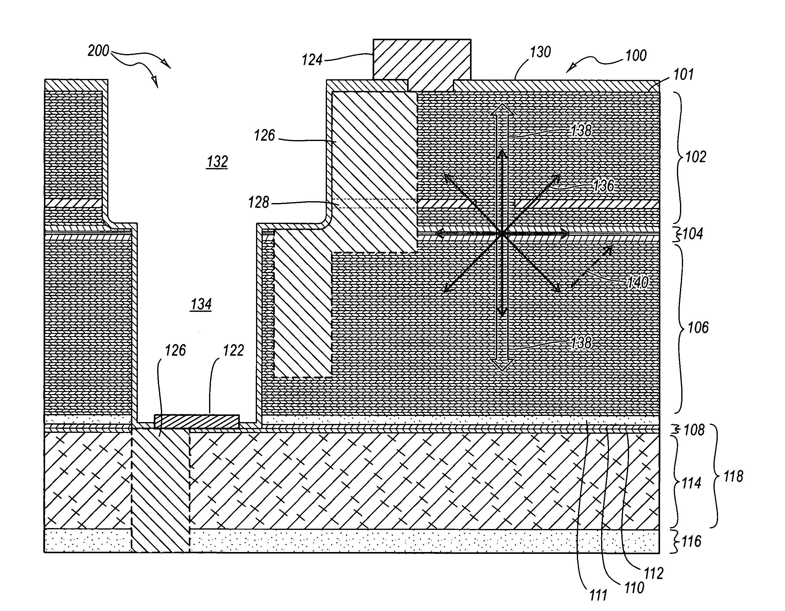
[0035]Embodiments described herein, implement various optimizations to reduce the amount of spontaneous emissions reaching a photodiode in an integrated VCSEL photodiode combination structure. Such optimizations include using absorbing layers at various portions of the structure, varying the geometry of the structure to change reflective angles, using optical apertures to the photodiode, changing the reflectivity of the mirror, changing the photodiode fabrication to be more impervious to spontaneous emissions at wavelengths different than the laser emissions, creating absorbing contacts, and using doping and implants to reduce photoluminescence caused by reemission of photons from absorbing materials.

[0036]An integrated photodiode and VCSEL structure will now be described with reference to FIG. 1. Notably, this example is simply one example of an integrated photodiode and VCSEL such as is described in U.S. Provisional Patent Application No. 10 / 877,915, titled “Light Emitting Device ...


PUM


Abstract

An optical structure that reduces the effects of spontaneous emissions from the active region of a laser. An optical structure includes optimizations to reduce the effects of spontaneous emissions. The optical structure includes a VCSEL with top and bottom DBR mirrors and an active region connected to the mirrors. The optical structure further includes a photodiode connected to the VCSEL. One or more optimizations may be included in the optical structure including optically absorbing materials, varying the geometry of the structure to change reflective angles, using optical apertures, changing the reflectivity of one or more mirrors, changing the photodiode to be more impervious to spontaneous emissions, and using ion implants to reduce photoluminescence efficiency.

Description

CROSS-REFERENCE TO RELATED APPLICATIONS[0001]This application is a continuation-in-part of U.S. application Ser. No. 10 / 877,915, titled “Light Emitting Device With an Integrated Monitor Photodiode” filed Jun. 25, 2004 now U.S. Pat. No. 7,184,454, which is incorporated herein by reference.BACKGROUND OF THE INVENTION[0002]1. The Field of the Invention[0003]The invention generally relates to integrated VCSEL and photodiode combinations. More specifically, the invention relates to methods and apparatuses for reducing the effects of spontaneous emissions from a VCSEL on an integrated photodiode.[0004]2. Description of the Related Art[0005]Lasers have become useful devices with applications ranging from simple laser pointers that output a laser beam for directing attention, to high-speed modulated lasers useful for transmitting high-speed digital data over long distances, to sensors for determining speed, distance, material compositions and the like. Several different types of lasers exis...

Claims


Application Information

Patent Timeline
Patent Type & Authority Patents(United States)
IPC IPC(8): H01S5/00H01S5/026H01S5/183
CPCH01S5/0264H01S5/18308H01S5/3095H01S5/0425H01S5/18311H01S5/18313H01S2301/02H01S5/18358H01S5/2022H01S5/2027H01S5/3054H01S5/1835H01S5/04257
Inventor GUENTER, JAMES K.TATUM, JIMMY A.BIARD, JAMES R.
Owner II VI DELAWARE INC
Why Eureka
Try Eureka