LED module, LED package, and wiring substrate and method of making same

a technology of led modules and wiring substrates, applied in the direction of metallic pattern materials, lighting and heating devices, lighting support devices, etc., can solve the problems of obstructing the low-profile led module or led package, and limited use, so as to enhance the reflection of light

Inactive Publication Date: 2012-01-05
SHINDO DENSHI KOGYO KK
View PDF2 Cites 76 Cited by
  • Summary
  • Abstract
  • Description
  • Claims
  • Application Information

AI Technical Summary

Benefits of technology

[0042]According to one embodiment of the invention, an LED module is constructed such that an LED chip is mounted on the surface of a buried plating (i.e., a heat dissipation metal filler formed in a via hole) opposite the mounting surface (on the side of a wiring pattern) of a conventional LED chip. In other words, in the embodiment of the invention, there is provided a wiring pattern on the side of the mounting surface of the LED chip. Therefore, it is not necessary to limit the kind of plating formed on the wiring pattern to silver though the wiring pattern is conventionally silver-plated to enhance the reflection of light from the LED chip on the wiring pattern.

Problems solved by technology

Since the wiring substrate using the above substrates 1) to 3) or the lead frame generally has a thickness of more than 200 μm, it may obstruct the low-profile LED module or LED package.
This use may be limited to the case that the LED chip is used at a large current for providing a lighter and more compact product or reducing the manufacturing cost.

Method used


Image

  • LED module, LED package, and wiring substrate and method of making same
  • LED module, LED package, and wiring substrate and method of making same
  • LED module, LED package, and wiring substrate and method of making same

Examples


first embodiment

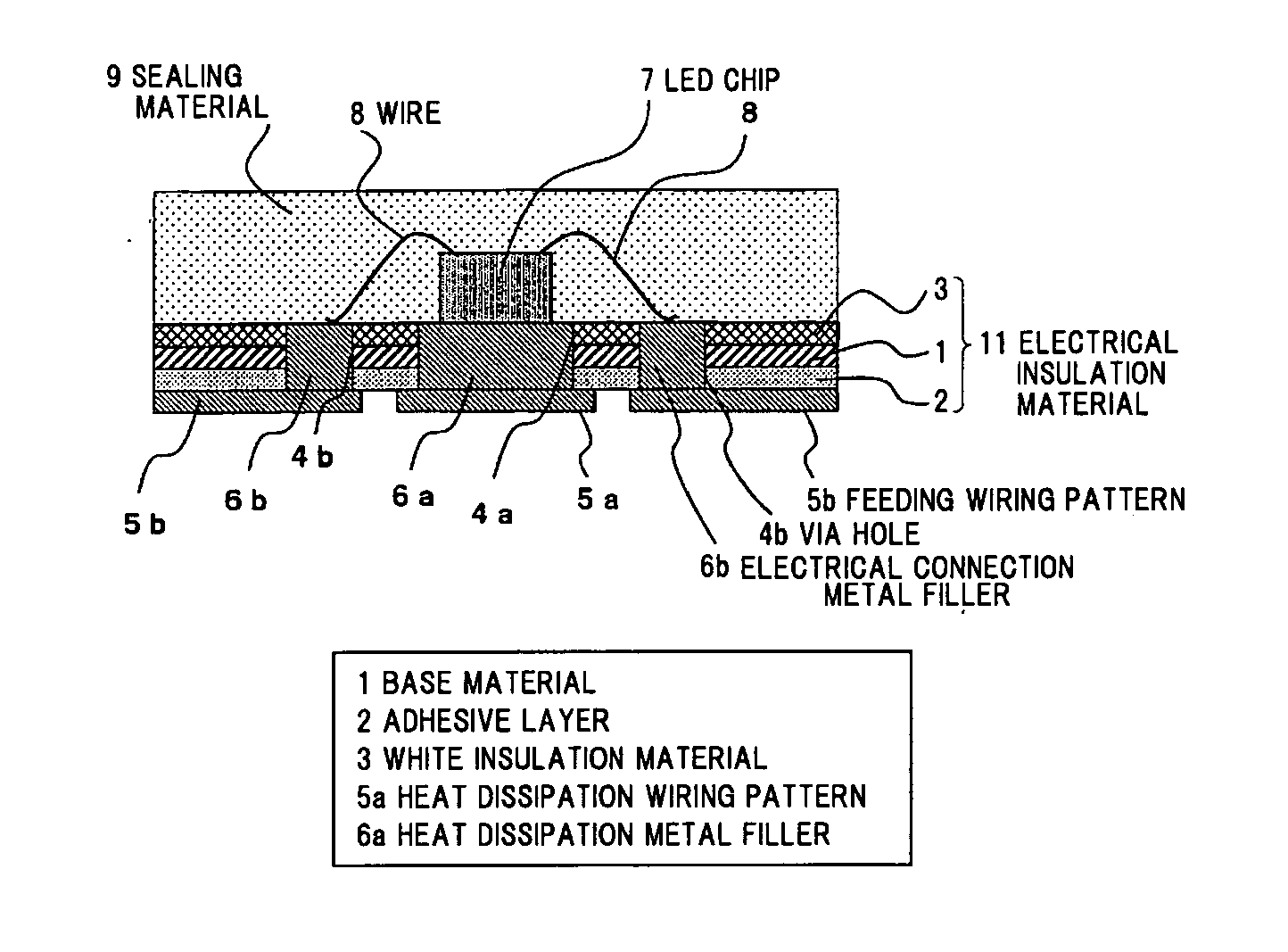
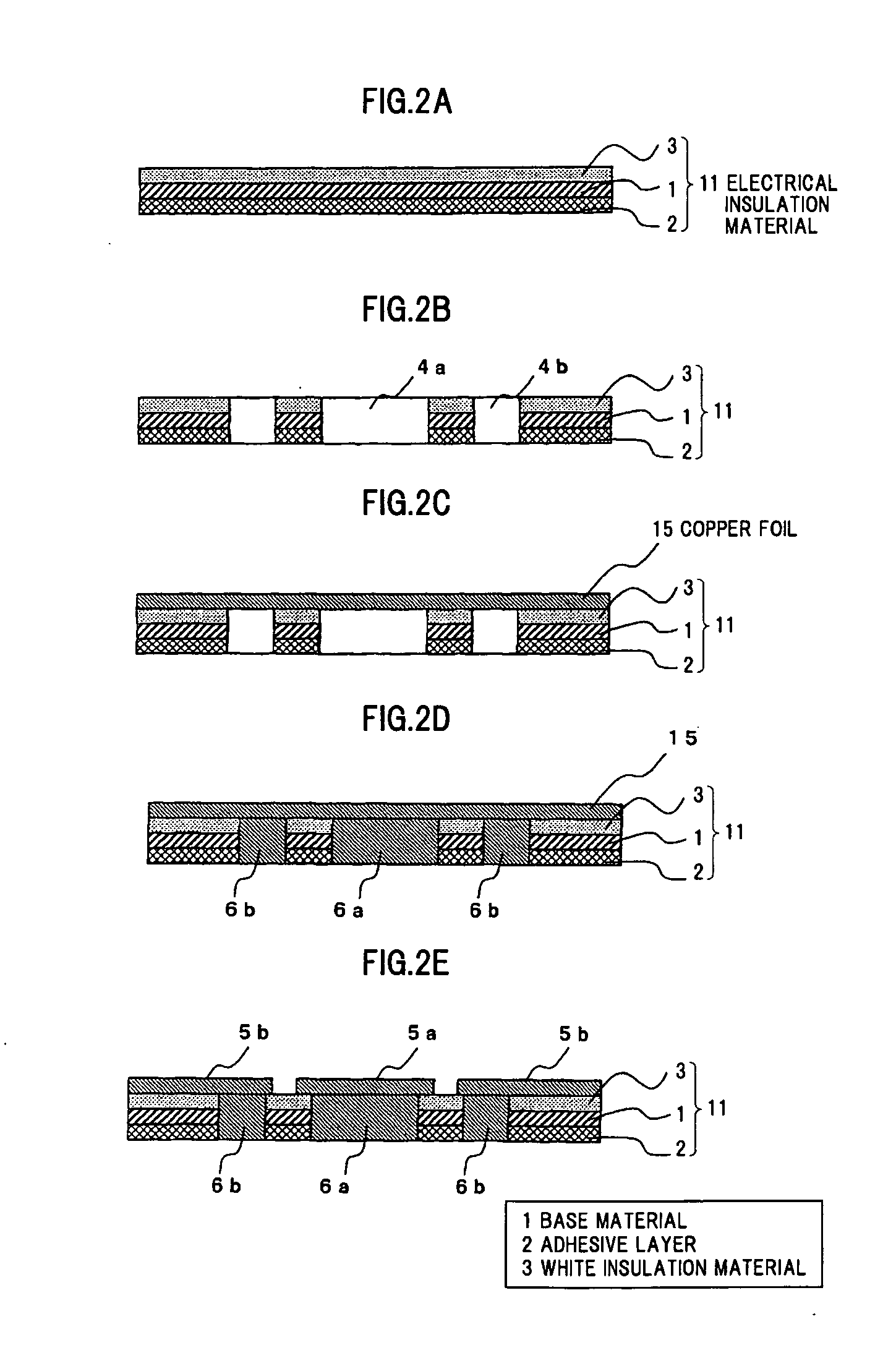
[0060]FIG. 1 is a cross sectional view showing one unit of an LED module in one embodiment of the invention. FIG. 2A to 2E are cross sectional views showing a method of making a wiring substrate in one embodiment of the invention. Although the method of the embodiment is exemplarily explained below in reference to a method of TAB (tape automated bonding) substrate, a method of making a rigid substrate or a flexible substrate etc. may also apply to the invention.

[0061]The LED module and wiring substrate in the embodiment are, as shown in FIG. 1, comprised of an electrical insulation material 11, via holes 4a, 4b penetrating through the electrical insulation material 11, a heat dissipation wiring pattern 5a, a feeding wiring pattern 5b, a heat dissipation metal filler 6a electrically connected to a wiring pattern formed in the via holes 4a, 4b, and a electrical connection metal filler 6b. An LED chip 7 is bonded on a first surface of the electrical insulation material 11 and to the ti...

second embodiment

[0087]FIGS. 7A to 7D show another embodiment of the invention. FIG. 7A is a cross sectional view showing one unit of an LED module using an LED chip capable of being flip-chip-mounted. FIG. 7B is a bottom view showing an example of a back pattern thereof.

[0088]The second embodiment is constructed such that the electrical connection metal filler 6b is formed in a via hole 4 of the electrical insulation material 11, and a bump 13 mounted on the LED chip 7 is directly electrically connected to the electrical connection metal filler 6b by using a flip-chip structure.

[0089]As shown in FIG. 7C, the electrical connection metal filler 6b of the via hole 4 may be higher than the surface of the electrical insulation material 11. Thereby, the sealing material becomes easy to fill without voids.

[0090]As shown in FIG. 7D, in order to facilitate the flip chip mounting (i.e., in order to secure the electrical connection between the bump 13 and the electrical connection metal filler 6b to reduce th...

third embodiment

[0091]FIGS. 8A and 8B show another embodiment of the invention. The third embodiment is constructed such that, in the second embodiment, a reflection portion 16 is formed molded with a white resin on the electrical insulation material 11, and the sealing material 9 is filled inside the reflection portion 16. FIG. 8A is a cross sectional view of one unit of the LED module and FIG. 8B is a top view thereof. In this embodiment, the simplest method of attaching the reflection portion 16 may be using a white sticky tape (not shown).

[0092]In FIG. 8A, the LED chip 7 is flip-chip mounted. As a matter of course, the LED chip 7 may be wire-bonded.


PUM

PropertyMeasurementUnit
reflectivityaaaaaaaaaa
thicknessaaaaaaaaaa
thicknessaaaaaaaaaa

Abstract

An LED module includes an electrical insulation material including a first surface having a total reflectivity of not less than 80% with respect to light with a wavelength of 450 nm, a via hole penetrating through the electrical insulation material, a wiring pattern on a second surface of the electrical insulation material, a metal filler formed in the via hole and electrically connected to the wiring pattern, and an LED chip bonded to a surface of the metal filler on the first surface of the electrical insulation material, and sealed with a resin.

Description

[0001]The present application is based on Japanese patent application Nos. 2010-151425, 2011-010341 filed on Jul. 1, 2010 and Jan. 21, 2011, respectively, the entire contents of which are incorporated herein by reference.BACKGROUND OF THE INVENTION[0002]1. Field of the Invention[0003]This invention relates to an LED module, an LED package, and a wiring substrate used for the LED module and the LED package, and a method of making the wiring substrate.[0004]2. Description of the Related Art[0005]In recent years, for the purpose of energy saving and CO2 emission reduction, products using an LED chip as a light source increase that include a mobile device with an LCD display such as a cellular phone and a laptop computer, an LCD television called “LED-TV” with an LED backlight, and an LED bulb using an LED module as a light source.[0006]These products have an LED module or an LED package installed therein that includes an LED chip mounted on a wiring substrate such as 1) a glass epoxy s...

Claims


Application Information

Patent Timeline
Patent Type & Authority Applications(United States)
IPC IPC(8): F21S4/00F21V21/00H01K3/10H05K1/09
CPCH01L33/46H01L33/486H01L33/54H01L33/60H01L33/62Y10T29/49165H01L2933/0033H01L2224/48227H01L33/64H01L2224/48235H01L2224/48091H01L2924/00014H01L33/48
Inventor IMAI, NOBORUNOGUCHI, MASAHIROISAKA, FUMIYASHIBATA, AKIJIASHIDATE, YUZURUSUZUKI, AKI
Owner SHINDO DENSHI KOGYO KK
Why Eureka
Try Eureka