Excimer laser apparatus projecting a beam with a selectively variable short-axis beam profile

a laser and selectively variable technology, applied in the direction of optical elements, instruments, manufacturing tools, etc., can solve the problems of waste of laser energy and small error margin for optimum energy density (oed)

Active Publication Date: 2015-01-20
COHERENT GMBH
View PDF11 Cites 7 Cited by
  • Summary
  • Abstract
  • Description
  • Claims
  • Application Information

AI Technical Summary

Problems solved by technology

The ELA process is a delicate process, and the error margin for the optimum energy density (OED) can be as small as 1%.
While the method of the '046 patent may be effective from the point of view of anticipating changes of OED with number of overlapping pulses, it is wasteful of laser energy.
Further, at the short wavelengths (less than 400 nm) of excimer laser radiation absorbers would be subject to damage, which at a minimum could alter the absorption values of the absorbers, and, accordingly, alter the step-profile.

Method used


Image

  • Excimer laser apparatus projecting a beam with a selectively variable short-axis beam profile
  • Excimer laser apparatus projecting a beam with a selectively variable short-axis beam profile
  • Excimer laser apparatus projecting a beam with a selectively variable short-axis beam profile

Examples


Embodiment Construction

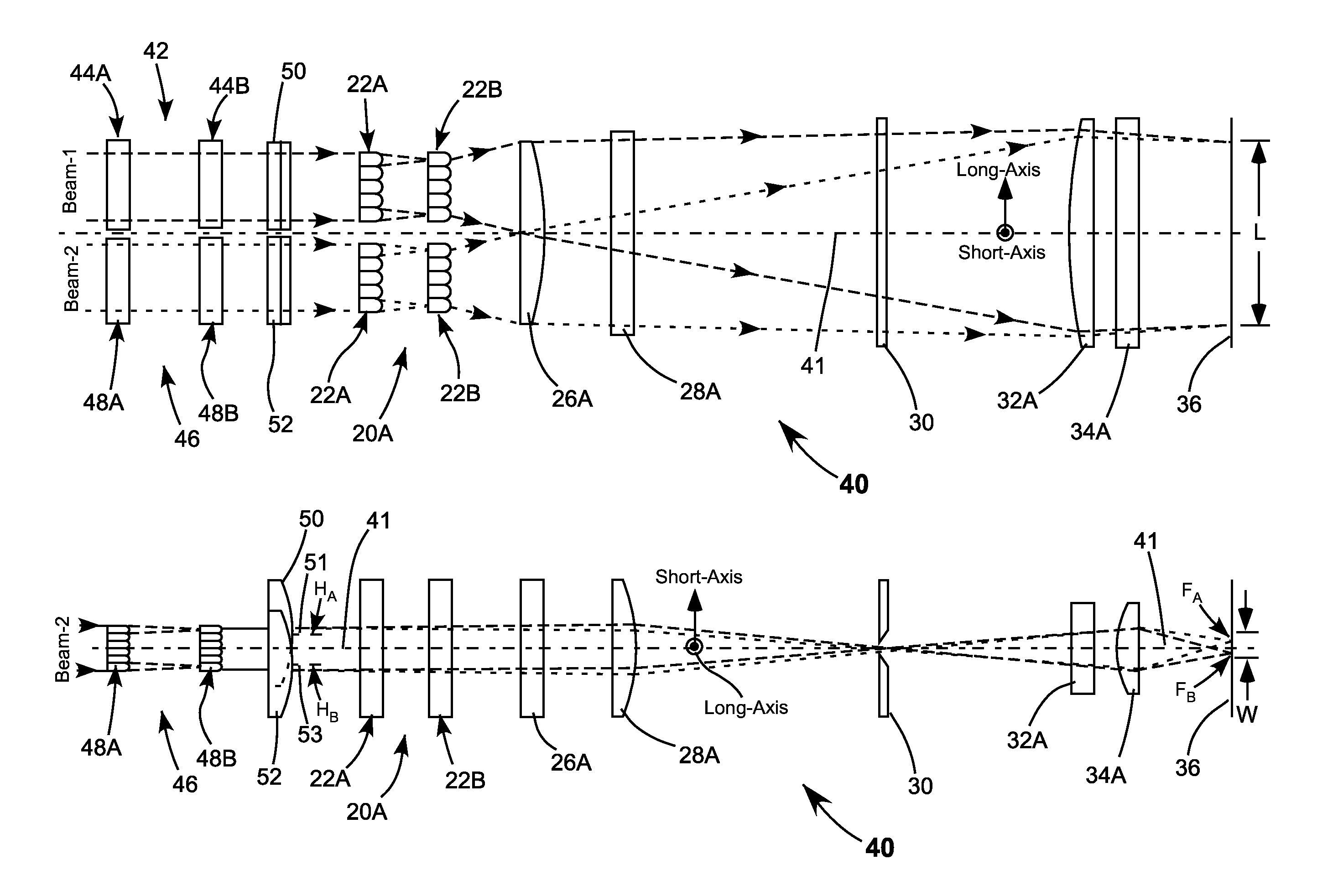
[0023]Referring now to the drawings, wherein like components are designated by like reference numerals, FIG. 3A and FIG. 3B are respectively long-axis and short-axis views schematically illustrating a preferred embodiment 40 of excimer-laser annealing apparatus in accordance with the present invention. Apparatus 40 has a system axis 41. Apparatus 40 is configured to accept two laser beams designated beam-1 and beam-2. The beams propagate parallel to each other spaced-apart in the long-axis direction of the apparatus and aligned one above the other in the short-axis direction of the apparatus.

[0024]The two beams can be beams from two separate excimer lasers or can be created by dividing a single input beam. Examples of two separate beams depicted in FIG. 5A, and FIG. 5B. Examples of creating two beams from a single beam are shown in FIG. 5C and FIG. 5D.

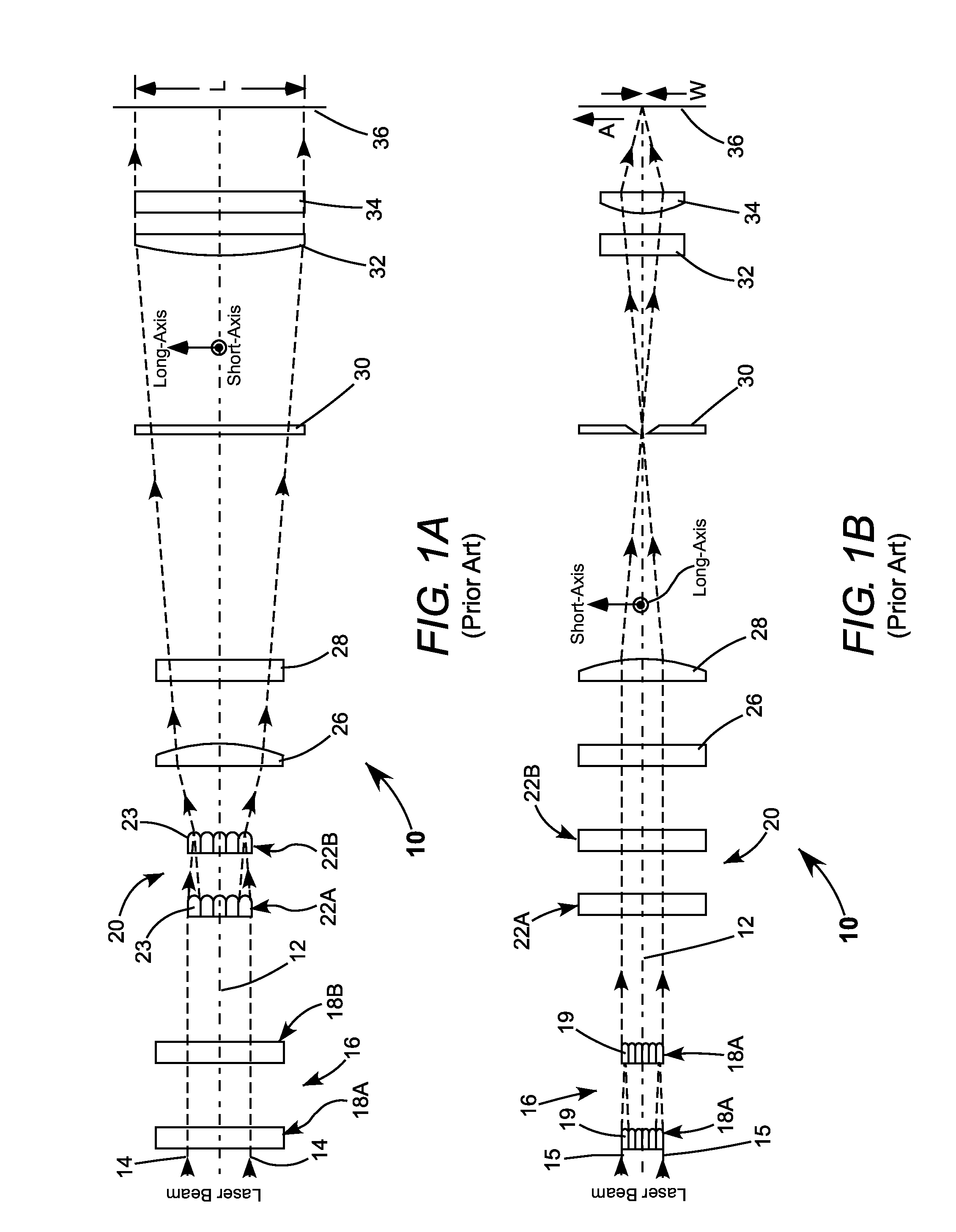
[0025]In the example of FIG. 5A there are simply two beams from two lasers, one beam from laser-1 and one beam from laser-2. These ca...


PUM

PropertyMeasurementUnit
lengthaaaaaaaaaa
lengthaaaaaaaaaa
widthaaaaaaaaaa

Abstract

Apparatus for homogenizing and projecting two laser-beams is arranged such that the projected homogenized beams are aligned parallel to each other in a first transverse axis and partially overlap in second transverse axis perpendicular to the first transverse axis. The projected homogenized laser-beams have different intensities in the second axis and the degree of partial overlap is selected such that the combined intensity of the laser beams in the second axis has a step profile.

Description

TECHNICAL FIELD OF THE INVENTION[0001]The present invention relates in general to melting and recrystallization of thin silicon (Si) layers by irradiation with laser-radiation beams. The method relates in particular to controlling the spatial profile of such beams.DISCUSSION OF BACKGROUND ART[0002]Silicon crystallization is a step that is often used in the manufacture of thin-film transistor (TFT) active-matrix LCDs, and organic LED (AMOLED) displays. The crystalline silicon forms a semiconductor base, in which electronic circuits of the display are formed by conventional lithographic processes. Commonly, crystallization is performed using a pulsed laser beam shaped in a long line. In this process, a thin layer of amorphous silicon on a glass substrate is repeatedly melted by pulses of laser radiation while the substrate (and the silicon layer thereon) is translated relative to a delivery source of the laser-radiation pulses. Melting and re-solidification (re-crystallization) throug...

Claims


Application Information

Patent Timeline
Patent Type & Authority Patents(United States)
IPC IPC(8): G02B27/09B23K26/00G02B13/08H01L21/02G02B27/10
CPCB23K26/0608B23K26/0648B23K26/0732B23K26/0676G02B27/095B23K26/0652B23K26/0081G02B27/09B23K2201/40B23K26/0042H01L21/02532H01L21/02686B23K26/0006B23K2101/40B23K2103/56B23K26/354
Inventor SIMON, FRANKVAN DER WILT, PAULSCHWENGER, LUDWIG
Owner COHERENT GMBH
Why Eureka
Try Eureka