Structure and antenna
a technology of structure and antenna, applied in the direction of resonant antennas, individual energised antenna arrays, line-transmission details, etc., can solve the problem of increasing manufacturing costs and achieve the effect of reducing the size and thickness of the antenna
- Summary
- Abstract
- Description
- Claims
- Application Information
AI Technical Summary
Benefits of technology
Problems solved by technology
Method used
Image
Examples
first embodiment
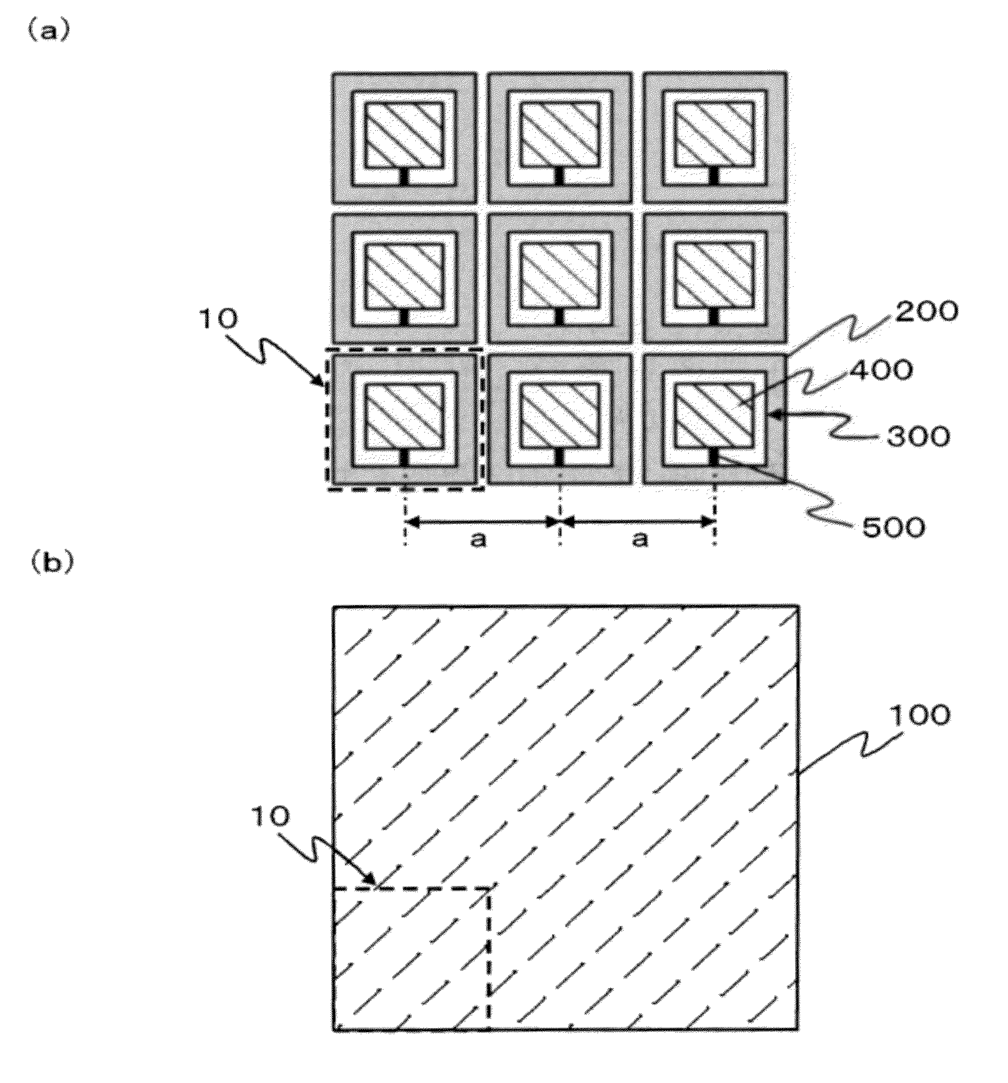
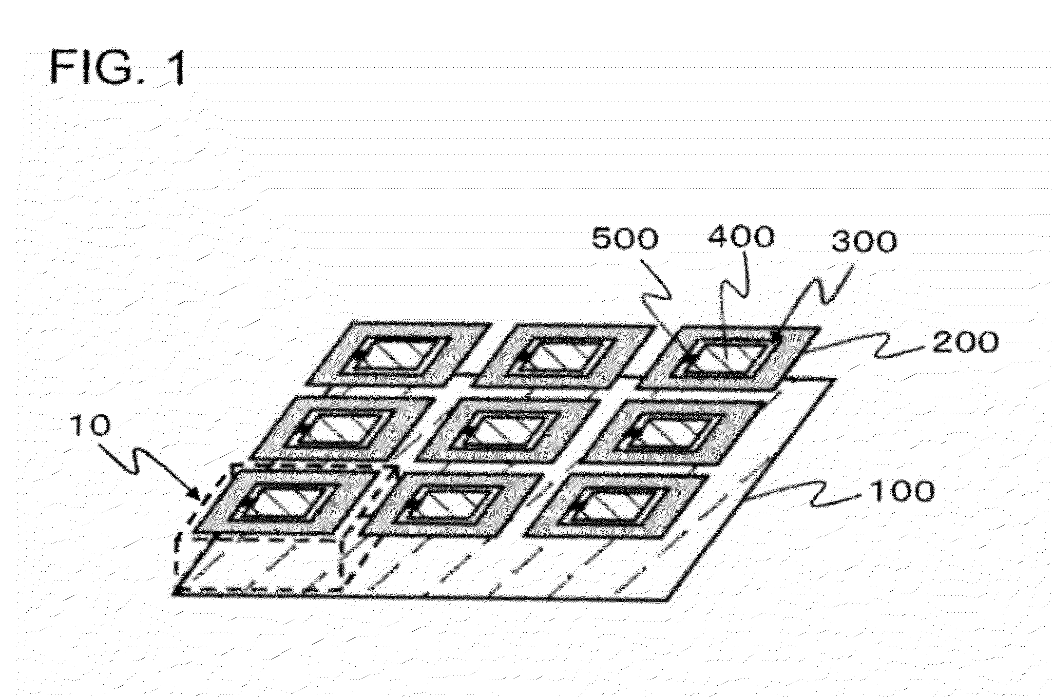
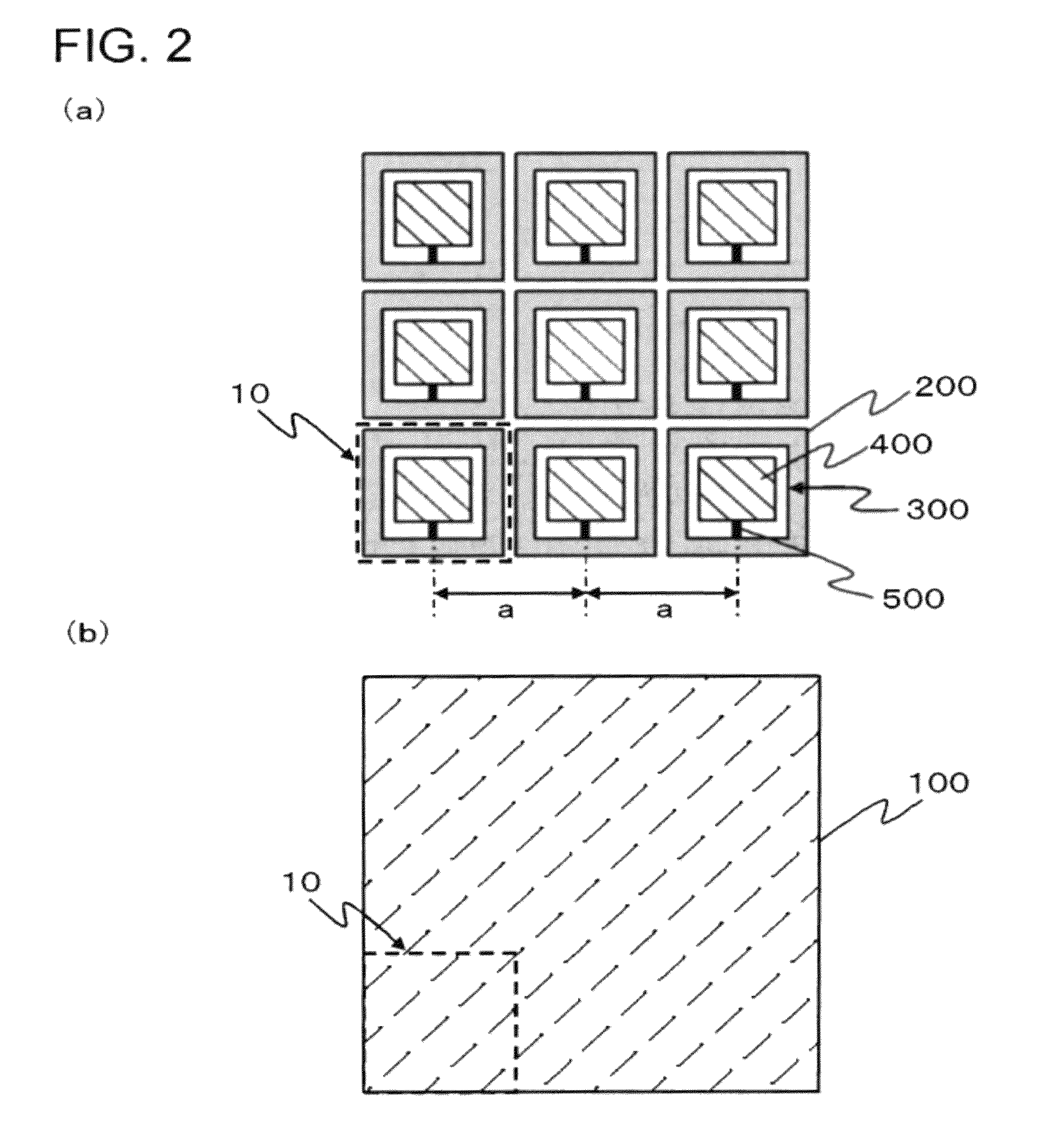
[0079]FIG. 1 is a perspective view illustrating a configuration of a structure according to a FIG. 2 (a) is a plan view illustrating a first layer of the structure shown in FIG. 1, and FIG. 2 (b) is a plan view illustrating a second layer of the structure shown in FIG. 1.
[0080]This structure includes a plurality of first conductor patterns 200 for a first conductor, a second conductor pattern 100 for a second conductor, openings 300, third conductor patterns 400 for a third conductor, and connection conductors 500. A plurality of first conductor patterns 200 are insular electrode patterns, are located at a first layer. The first conductor patterns 200 are arranged in a repetitive pattern, for example, in a periodic pattern and are separated from each other. The second conductor pattern 100 is located at a second layer parallel to the first layer. At least a portion of the second conductor pattern 100 is provided in a region opposite a plurality of first conductor patterns 200. In t...
eleventh embodiment
[0122]FIG. 18 is a diagram illustrating a second modified example of the structure shown in FIG. 15. This structure has a configuration in which the structure is provided with the fourth conductor pattern 600 shown in FIG. 15. That is, this structure has the same configuration as that of the structure shown in FIG. 15, except that the second conductor pattern 100 is provided with the opening 300, the third conductor pattern 400, and the connection conductor 500. An equivalent circuit in the modified example is also the same as the equivalent circuit shown in FIG. 16.
[0123]Each drawing of FIG. 19 is a diagram illustrating a third modified example of the structure shown in FIG. 15. This structure has a planar shape of the fourth conductor pattern 600 different from that in the example shown in FIG. 15. In the example shown in FIG. 19(a), the fourth conductor pattern 600 is rhombic, and overlaps the center of any of the sides of the first conductor pattern 200. In addition, in the exa...
fifth embodiment
[0124]FIG. 20 is a diagram illustrating a fourth modified example of the structure shown in FIG. 15. This structure has a configuration in which the structure is provided with the fourth conductor pattern 600. The fourth conductor patterns 600 are regular hexagonal. Each of the fourth conductor patterns 600 is formed to overlap three first conductor patterns 200 of which the tops are adjacent to each other, and these overlapping areas are the same in size as each other.
[0125]According to the embodiment, as shown in two drawings of FIG. 16, the capacitive component between two first conductor patterns 200 adjacent to each other increases. For this reason, it is possible to adjust the meta-material characteristics of the structure in a wider range.
[0126]Meanwhile, in the first to fifth embodiments and the seventh to twelfth embodiments, there may be a portion not including the unit cells 10, and for example, as shown in FIGS. 21 and 22, the structure may be configured to have a latti...
PUM
 Abstract
Description
Claims
Application Information


