Semiconductor package, substrate, electronic device using such semiconductor package or substrate, and method for correcting warping of semiconductor package

a technology applied in the direction of printed circuits, printed circuit manufacturing, basic electric elements, etc., can solve the problems of defective connections, substrates, and reduced thickness of semiconductor packages. , to achieve the effect of preventing defective solder connections, reducing warping, and reducing dead area

Inactive Publication Date: 2009-11-26
NEC CORP
View PDF22 Cites 17 Cited by
  • Summary
  • Abstract
  • Description
  • Claims
  • Application Information

AI Technical Summary

Benefits of technology

[0020]In the semiconductor package configured as described above, the inflection point forming portion can generate stress in a direction opposite to warping which occurs due to a difference in the coefficient of thermal expansion between the semiconductor chip and the substrate as a thermal load occurs during solder reflow. Thus, inflection points occur when the substrate warps at solder reflow temperatures. In this way, since a connection area, which is particularly required to be horizontal, can be made parallel to another substrate to be connected, defective solder connections are prev

Problems solved by technology

As a result, semiconductor packages tend to increase in size.
The warping of semiconductor packages which accompanies such a reduction in thickness of semiconductor packages and substrates has become problematic.
If the interstice between the other substrate and the solder balls cannot be filled with cream solder which is supplied to the solder balls and other substrate and even if which is melted therein, defective connections arise.
As such, the center of the side is particularly susceptible to a defective connection.
well. In this way, though the warping state is different from the structure shown in FIGS. 1 and 2, defective connections arise if the interstice between the other substrate and the solder balls is not filled with cream solder which is supplied to the solder balls and other substrate and even if which is
Thus, defective connections due to warping have become increasingly prominent.
However, particularly when semiconductor chip 1 has a thickness of 0.3 mm or less, or when substrate 2 has a thickness of 0.8 mm or less, promin

Method used


Image

  • Semiconductor package, substrate, electronic device using such semiconductor package or substrate, and method for correcting warping of semiconductor package
  • Semiconductor package, substrate, electronic device using such semiconductor package or substrate, and method for correcting warping of semiconductor package
  • Semiconductor package, substrate, electronic device using such semiconductor package or substrate, and method for correcting warping of semiconductor package

Examples


Embodiment Construction

[0076]In the following, embodiments of the present invention will be described with reference to the drawings.

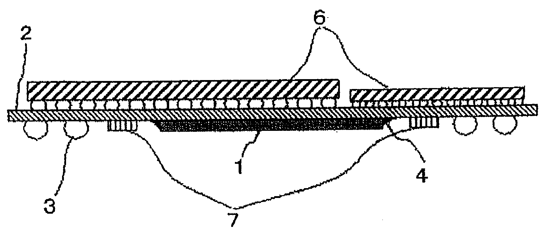
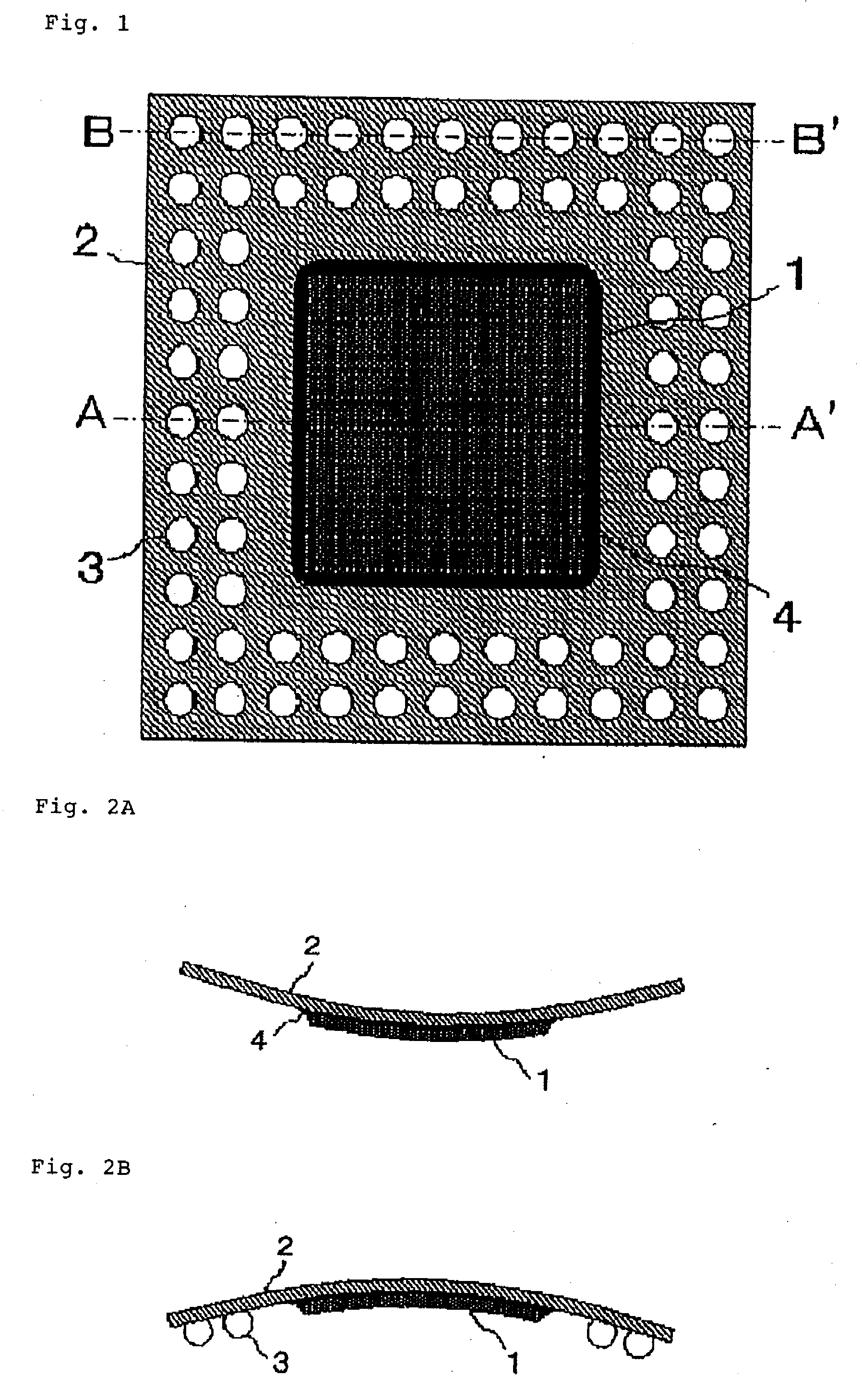
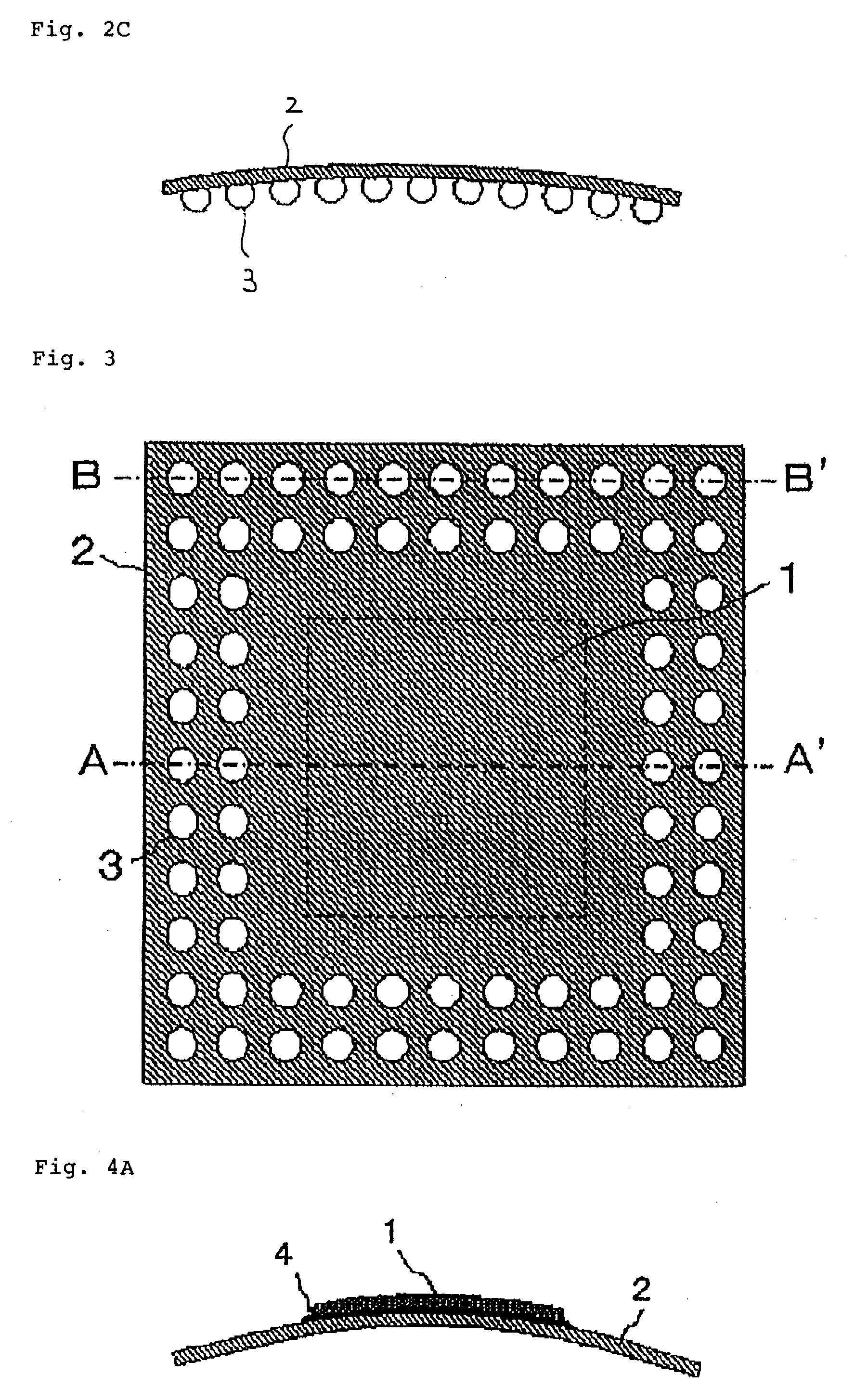
[0077]A semiconductor package of the present invention has a semiconductor chip mounted on one surface of a substrate, where an inflection point forming portion is formed in a part of the surface on which the semiconductor chip is mounted. This substrate warps due to the difference in the coefficient of thermal expansion between the semiconductor chip and the substrate. The inflection point forming portion is made of a material which is capable of generating warping in the direction opposite to the warping. In this way, since a connection area can be nearly horizontal during solder reflow, defective solder connections can be restrained when this semiconductor package is connected to another substrate. A material for forming the inflection point forming portion used herein can be a material having a larger coefficient of thermal expansion than a material which comprises the s...


PUM


Abstract

Disclosed is a semiconductor package wherein a semiconductor chip is mounted on one surface of a substrate. In this semiconductor package, an inflection point forming portion made of a material having a higher coefficient of thermal expansion than the substrate is formed in a part of the substrate surface on which the semiconductor chip is mounted.

Description

TECHNICAL FIELD[0001]The present invention relates to a semiconductor package, and a substrate used in this semiconductor package. Particularly, the present invention relates to a semiconductor package which has a semiconductor chip mounted on a substrate by a flip-chip method. Also, the present invention relates to an electronic device which uses the substrate or semiconductor package. Further, the present invention relates to a method for correcting warping of such a semiconductor package.BACKGROUND ART[0002]With increasing reductions in size and thickness of portable terminals, semiconductor packages are required to be reduced in size and thickness. To meet such requirements, there is an increased need for semiconductor packages which apply a flip-chip connection technology. The flip-chip connection technology, herein referred to, is a technology which involves providing terminals on a circuit surface of a semiconductor chip, and directly connecting these terminals to pads on a s...

Claims


Application Information

Patent Timeline
IPC IPC(8): H01L23/12H05K1/03H01L21/26
CPCH01L23/16H01L23/3128H01L2924/16251H01L2924/15321H01L2924/15311H01L2224/73204H01L2224/32225H01L2224/16225H05K3/3436H05K1/0271H01L23/49816H01L23/562H01L2924/3511H01L2924/00
Inventor WATANABE, SHINJI
Owner NEC CORP
Why Eureka
Try Eureka