Plasma dicing apparatus and method of manufacturing semiconductor chips

a technology of plasma dicing and semiconductor chips, applied in the direction of individual semiconductor device testing, semiconductor/solid-state device testing/measurement, instruments, etc., can solve problems such as poor workability, and achieve the effect of very easy handling

Inactive Publication Date: 2010-02-25
PANASONIC CORP
View PDF5 Cites 211 Cited by
  • Summary
  • Abstract
  • Description
  • Claims
  • Application Information

AI Technical Summary

Benefits of technology

[0006]The present invention provides a plasma dicing apparatus facilitating carrying a semiconductor wafer into and out of the vacuum chamber to improve workability and a method of manufacturing semiconductor chips using the plasma dicing apparatus.
[0008]With such a structure, the outer circumference of the etching-resistant mask member stuck onto the back surface (opposite to the circuit-forming surface) of the semiconductor wafer is retained by a ring-shaped frame member. Further, the vacuum chamber is provided therein with a frame member supporting part supporting the frame member on the outer circumference of the wafer supporting part supporting the semiconductor wafer. Consequently, the semiconductor wafer can be handled in a state unified with the mask member retained by the frame member before and after the plasma dicing process in the vacuum chamber. Hence, when carrying the semiconductor wafer into and out of the vacuum chamber, the mask member retained by the frame member can be made function as a transfer carrier for the semiconductor wafer. That is, the structure facilitates carrying a semiconductor wafer into and out of the vacuum chamber to improve workability.
[0010]With such a structure, a semiconductor wafer stays in a state of the mask member retained by the frame member stuck at least after the masking step to the die bonding sheet sticking step. Further, the mask member retained by the frame member is used as a transfer carrier for the semiconductor wafer and the semiconductor chips diced in the plasma dicing step. As a result, a semiconductor wafer can be handled very easily between each step. Here, the mask member is attached to the back surface of a semiconductor wafer after the semiconductor wafer undergoes the thinning step. Hence, the frame member does not interfere with a grinding tool as before, allowing an existing facility to be used in the thinning step.

Problems solved by technology

However, a semiconductor wafer is extremely vulnerable such as to shock before being diced into individual semiconductor chips by plasma dicing, which requires careful handling when carrying the semiconductor wafer into and out of the vacuum chamber, which causes poor workability.[Patent literature 1] Japanese Patent Unexamined Publication No. 2005-191039

Method used


Image

  • Plasma dicing apparatus and method of manufacturing semiconductor chips
  • Plasma dicing apparatus and method of manufacturing semiconductor chips
  • Plasma dicing apparatus and method of manufacturing semiconductor chips

Examples


Embodiment Construction

[0095]Hereinafter, a description is made of an exemplary embodiment of a plasma dicing apparatus and a method of manufacturing semiconductor chips by means of the plasma dicing apparatus, of the present invention, in reference to related drawings.

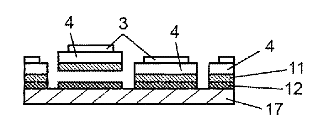
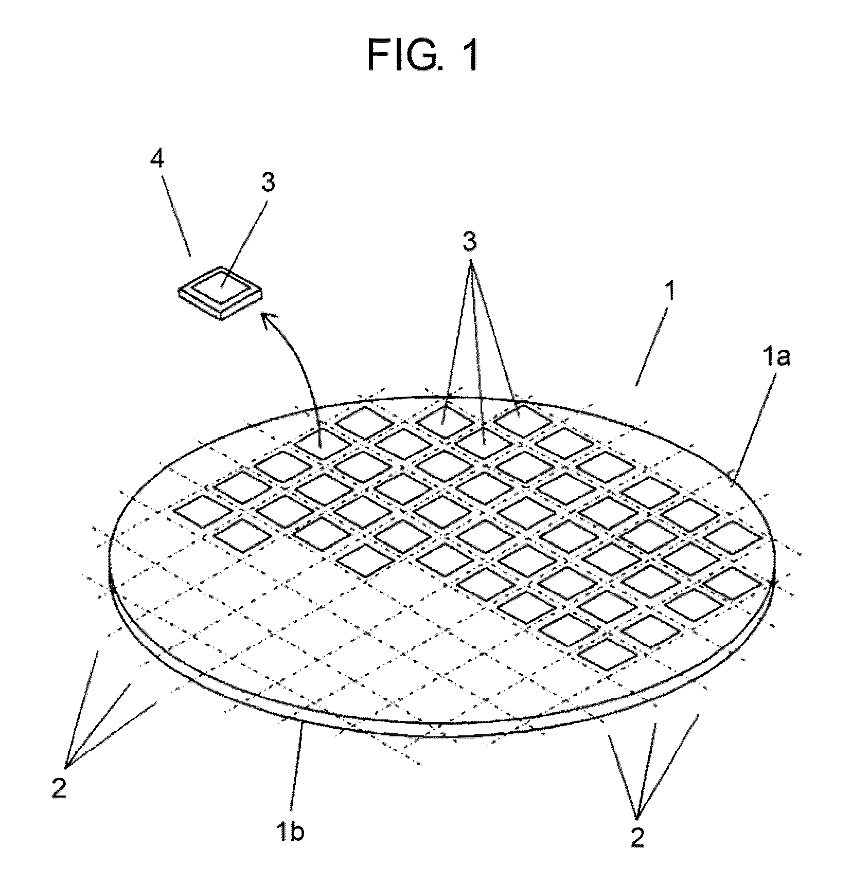
[0096]FIG. 1 is a perspective view showing a semiconductor wafer used in an embodiment of the present invention. In FIG. 1, circuit-forming surface 1a on the top surface of semiconductor wafer 1 is partitioned into plural areas by lattice-shaped streets (dicing line) 2, and each area partitioned has semiconductor element (integrated circuit) 3 formed thereon. Accordingly, semiconductor wafer 1, if diced along street 2, produces a large number of semiconductor chips 4 collectively. The method of manufacturing semiconductor chips by means of a plasma dicing apparatus according to the embodiment produces semiconductor chips 4 from semiconductor wafer 1 shown in FIG. 1.

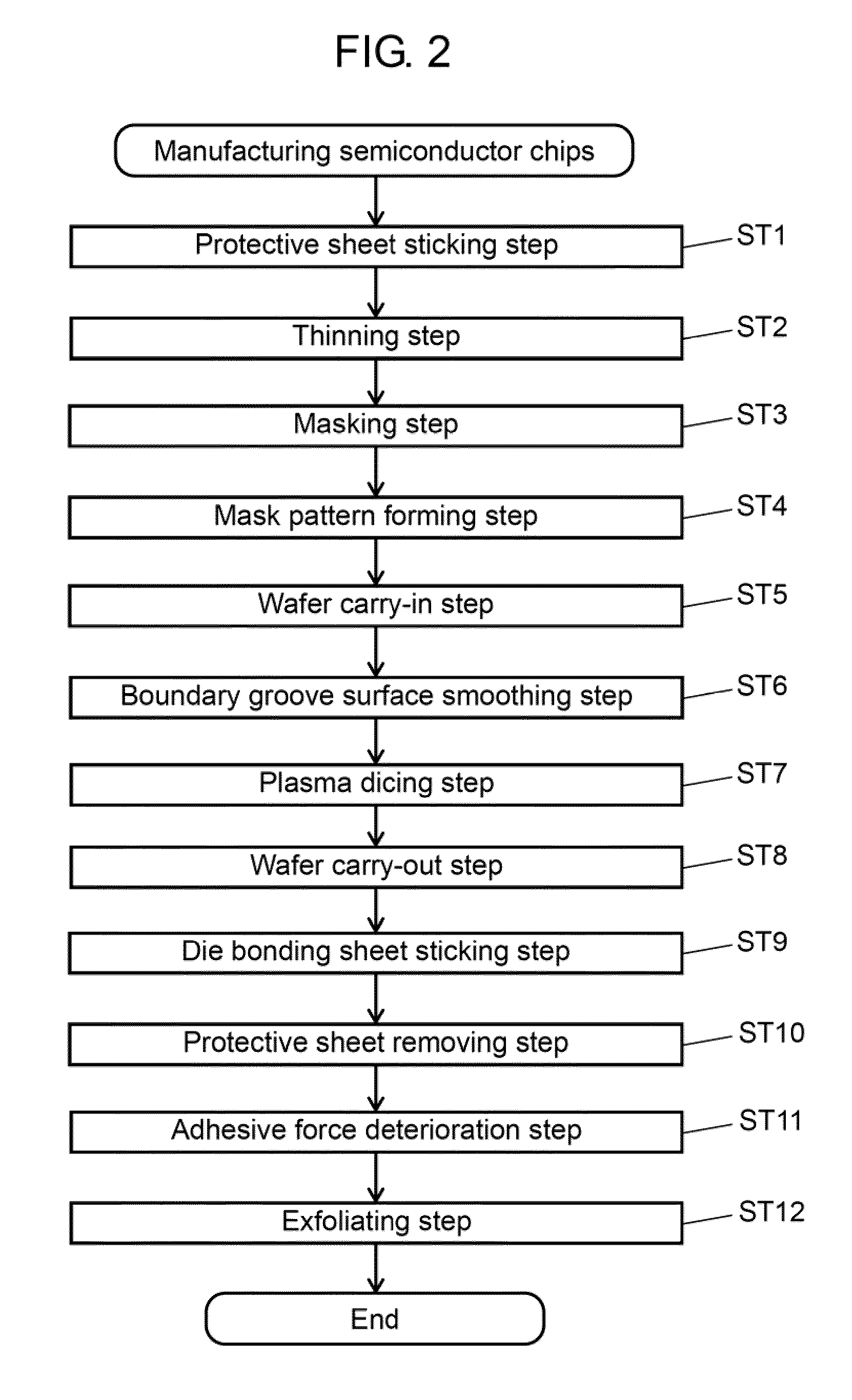
[0097]FIG. 2 is a flowchart showing the method of manufacturing semiconducto...


PUM

PropertyMeasurementUnit
thicknessaaaaaaaaaa
stress concentrationaaaaaaaaaa
circumferenceaaaaaaaaaa

Abstract

A plasma dicing apparatus in which a semiconductor wafer with a protective sheet stuck thereonto covering the entire circuit-forming surface and with an etching-resistant mask member stuck on the back surface opposite to the circuit-forming surface is mounted on a mounting stage; plasma etching is performed using the mask member as a mask; and the semiconductor wafer is diced into plural semiconductor chips. The plasma dicing apparatus includes a ring-shaped frame member retaining the outer circumference of the mask member extending off the outer circumference of the semiconductor wafer. The mounting stage is composed of a wafer supporting part supporting a semiconductor wafer and a frame member supporting part supporting the frame member. This facilitates carrying a semiconductor wafer into and out of the vacuum chamber.

Description

TECHNICAL FIELD[0001]The present invention relates to a plasma dicing apparatus that performs plasma etching on a semiconductor wafer in a vacuum chamber and dices the semiconductor wafer into individual semiconductor chips, and to a method of manufacturing semiconductor chips.BACKGROUND ART[0002]A semiconductor chip implemented such as on a board of an electronic appliance is produced by dicing a semiconductor wafer partitioned by streets (dicing line), along the streets. As a method of dicing a semiconductor wafer, a mechanical method using a dicing saw is known. Besides, in recent years, plasma dicing, which is a method of cutting off by plasma etching, has been devised (patent literature 1).[0003]In such a method of manufacturing semiconductor chips using plasma dicing, a sheet-like supporting member (protective sheet) is first stuck onto the circuit-forming surface of a semiconductor wafer so as to cover the entire circuit-forming surface, and then a mask layer (mask member) wi...

Claims


Application Information

Patent Timeline
Patent Type & Authority Applications(United States)
IPC IPC(8): H01L21/302H01L21/3065
CPCH01J37/32743H01J37/32788H01L21/78H01L21/308H01L21/67069H01L21/3065
Inventor HARIKAI, ATSUSHIARITA, KIYOSHIIWAI, TETSUHIRO
Owner PANASONIC CORP
Why Eureka
Try Eureka