Diode housing

a diode housing and diode technology, applied in the field of diode housings, can solve the problems of temperature variations in the operating environment of the housing, reducing the amount of radiation being emitted from or incident,

Inactive Publication Date: 2003-09-23
OSRAM GMBH
View PDF21 Cites 209 Cited by
  • Summary
  • Abstract
  • Description
  • Claims
  • Application Information

AI Technical Summary

Problems solved by technology

A drawback with the above discussed arrangements, as briefly alluded to in the prior art reference, stems from the delamination of the window 110 carrier frame 103.
Such delaminating may result from temperature variations in the housing's operating environment, such as proximate to an automobile engine or manufacturing (e.g. soldering) requirements.
Such gaps result in radiation absorption and / or internal reflections thereby diminishing the amount of radiation being emitted from or incident to chip 101.

Method used


Image

  • Diode housing
  • Diode housing
  • Diode housing

Examples


Embodiment Construction

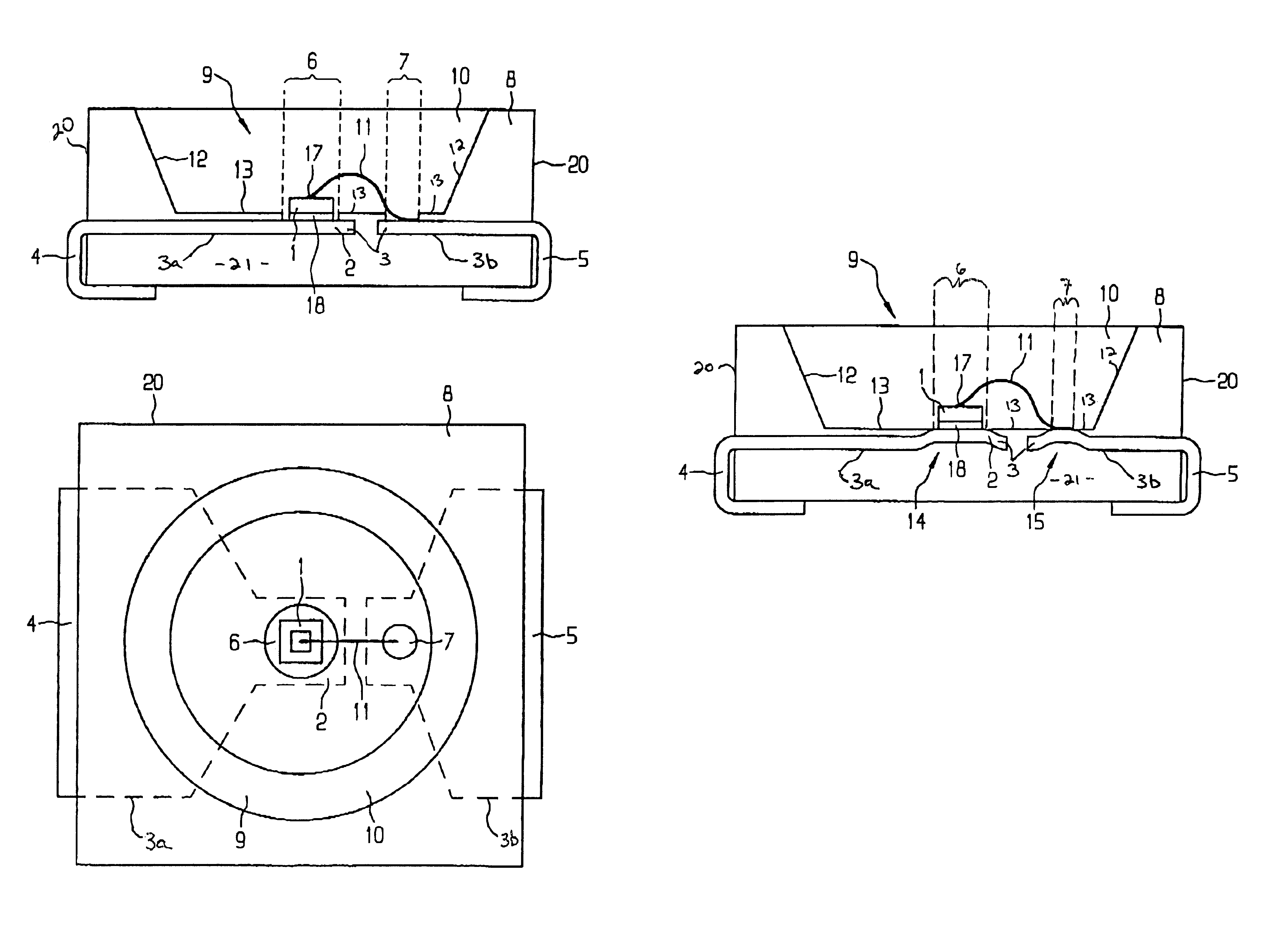
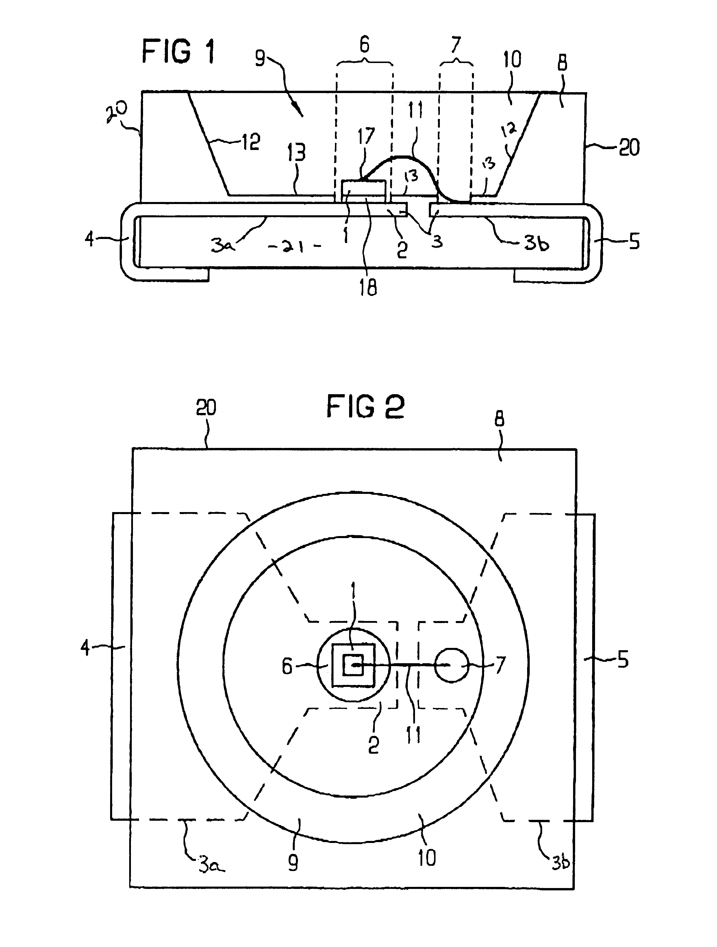
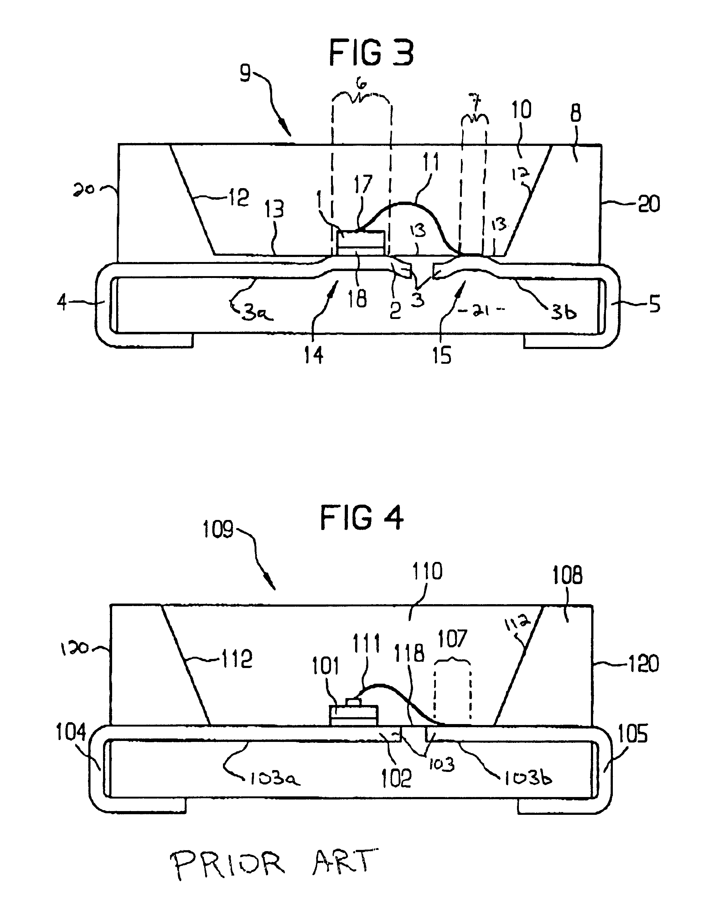
Reference is now made to the figures of the drawings in which elements that are identical or that function identically are identified by the same reference numerals throughout. FIGS. 1 and 2 set out the first embodiment of the present invention which comprises an LED component part for use in SMT or related technology. The component comprises a lead frame 3, accommodating a semiconductor chip 1 on a first conductor portion 3a and a first end of wire 11 is bonded to a second conductor portion 3b. A second end of wire 11 is bonded 17 to semiconductor 1. A housing 20, made of synthetic materials known to one skilled in the art, accommodates the conductor, chip and wire. Portion 3a extends outwards from and around a base 21 of housing 20 thereby forming external conductor 4. Likewise, second conductor 3b extends outwards from and around the base 21 of housing 20 thereby forming external conductor 5. A top of the component is formed by the housing 20 and an opening therein and cavity 9 e...


PUM


Abstract

A housing accommodating a semiconductor chip is set out. The housing and chip may be used for sending and / or receiving radiation. Popular applications of the housing may be in light emitting diodes. The housing includes a conductor strip that is punched into two electrically isolated portions. The housing further includes a cavity extending inwards from the top of the housing. The conductor portions include respective areas that are exposed at the bottom of the cavity. The semiconductor chip is bonded to one of the exposed areas and a wire bonds the chip to the second exposed area. The conductor portions also terminate in exposed electrodes, which allow for electrical connection of the chip with external devices. A window is formed in the cavity and the walls of the housing that form the cavity may be made of a reflective material. The electrodes remain unexposed to the window but for any residual areas about the chip and bonding wire within the first and second exposed areas. By minimizing the area of the conductor exposed to the window, delamination brought about by the different thermal expansions of the window and conductor are minimized and / or eliminated. Likewise, with a reflective housing covering the base of the cavity that accommodates the window, internal radiation reflection is increased over that which was achieved with an exposed conductor.

Description

1. Field of the InventionThe present invention relates to the field of optoelectronic components and more particularly to an improved housing design for a radiation sending and / or receiving device. Such device may comprise one or more optoelectronic chips, which are generally mounted on a chip supporting part of an electrical lead frame running through a base body. Common applications for such chips may include light emitting diodes (LED).2. Description of Related ArtHousings for radiation sending and / or receiving devices are generally well known in the art. An example of prior art housings is set out in an article "Siemens-SMT-TOP-LED-LED's for Surface Mounting", Siemens Components XXVI (1991), Nos. 4-5, pages 147 to 149. This article is herein incorporated by reference. The article discusses the state of the art, as of 1991, of surface mounted TOP LED's. A side by side comparison of TOP and radial LEDs is set out in FIG. 4 of the article. A perspective view of a TOP LED is shown i...

Claims


Application Information

Patent Timeline
Patent Type & Authority Patents(United States)
IPC IPC(8): H01L33/00H01L31/02H01L31/0203H01L33/48H01L33/62
CPCH01L31/0203H01L33/486H01L24/45H01L33/62H01L2224/32245H01L2224/45144H01L2224/48091H01L2224/48247H01L2224/48465H01L2224/73265H01L2924/01058H01L2924/01079H01L2924/00014H01L2924/01019H01L2924/12041H01L2924/00H01L2924/181
Inventor WAITL, GUNTHERBRUNNER, HERBERT
Owner OSRAM GMBH
Why Eureka
Try Eureka