Stack package having guard ring which insulates through-via interconnection plug and method for manufacturing the same

a technology of guard ring and interconnection plug, which is applied in the field of stack packages, can solve the problems of joint reliability deterioration, cracks and disconnections likely to be produced at the joint regions between the connection, and achieve the effect of preventing cracks and disconnections

Active Publication Date: 2009-04-28
SK HYNIX INC
View PDF9 Cites 209 Cited by
  • Summary
  • Abstract
  • Description
  • Claims
  • Application Information

AI Technical Summary

Benefits of technology

[0009]The present invention is directed to a stack package in which chips are connected by connection plugs filling through-vias while allowing relaxation of a stress upon a thermal cycle test to thereby prevent cracks and disconnections from being produced at joint regions between the chips, and a method for manufacturing the same.
[0010]Also, the present invention is directed to a stack package which prevents cracks and disconnections from being produced at joint regions between chips, thereby improving the reliability of a solder joint, and a method for manufacturing the same.

Problems solved by technology

In this type of conventional stack package in which the chips are connected with each other using the through-via interconnection plugs, when performing a thermal cycle reliability test, cracks and disconnections are likely to be produced at joint regions between the connection plugs, because of thermal expansion and contraction.
As a result, joint reliability deteriorates.
Since joint reliability deteriorates, device reliability deteriorates.

Method used


Image

  • Stack package having guard ring which insulates through-via interconnection plug and method for manufacturing the same
  • Stack package having guard ring which insulates through-via interconnection plug and method for manufacturing the same
  • Stack package having guard ring which insulates through-via interconnection plug and method for manufacturing the same

Examples


Embodiment Construction

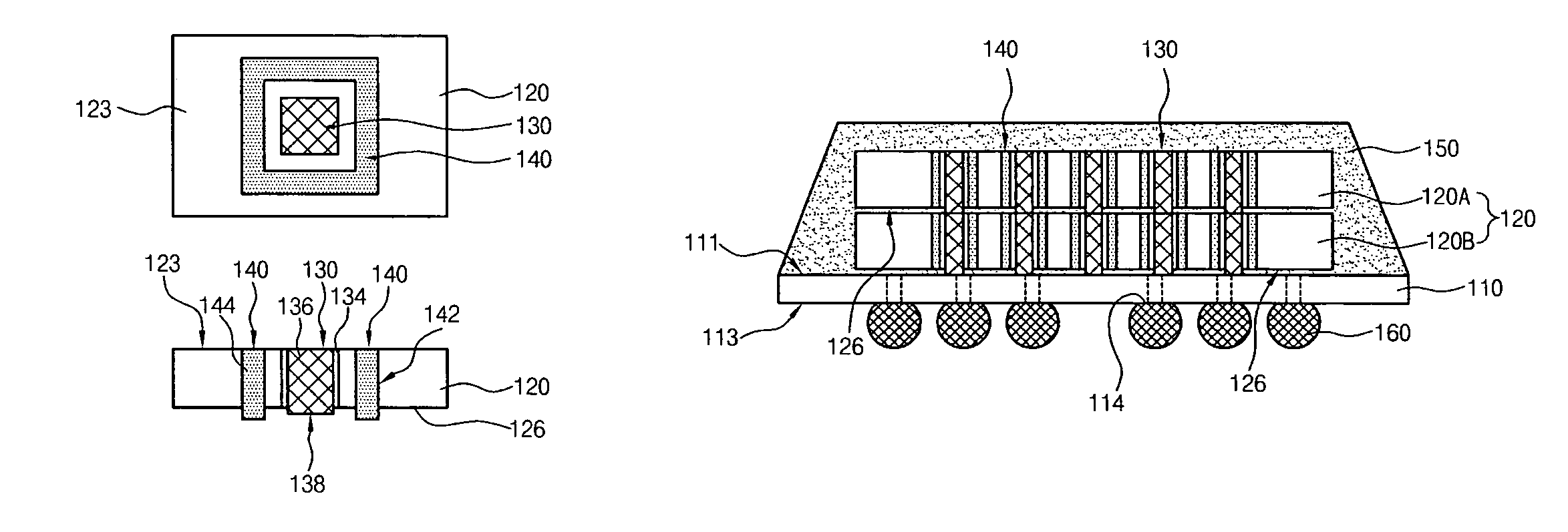
[0025]In the present invention, when manufacturing a stack package, a stack of two or more semiconductor chips is formed using electrically conductive through-via interconnection plugs. The through-vias extend through at least one of the semiconductor chips to be stacked and enable the two stacked semiconductor chips to be electrically coupled to each other. The through vias are surrounded by guard rings which absorb thermally-induced stresses and which provide an electrical insulation around the respective through-via interconnection plugs.

[0026]In a stack package, the guard ring electrically insulates a through-via interconnection pattern and the inside of a chip from each other. The guard ring reduces or eliminates thermally-induced stress that can be concentrated on the through-via interconnection plug when the chip's temperature fluctuates. The guard ring prevents stress from being concentrated on the through-via interconnection plug and reduces or eliminates cracks in a semico...


PUM


Abstract

A stack package comprises a substrate having a circuit pattern; at least two semiconductor chips stacked on the substrate, having a plurality of through-via interconnection plugs and a plurality of guard rings which surround the respective through-via interconnection plugs, and connected with each other by the medium of the through-via interconnection plugs; a molding material for molding an upper surface of the substrate including the stacked semiconductor chips; and solder balls mounted to a lower surface of the substrate.

Description

CROSS-REFERENCE TO RELATED APPLICATIONS[0001]The present application claims priority to Korean patent application number 10-2006-0096717 filed on Sep. 30, 2006, which is incorporated by reference in its entirety.BACKGROUND OF THE INVENTION[0002]The present invention relates to a stack package, and more particularly, to a stack package which is realized using a through-via interconnection plug and a method for manufacturing the same.[0003]In the semiconductor industry, packaging technology for an integrated circuit has continuously been developed to meet the demand toward miniaturization and mounting reliability. Recently, as the miniaturization and high functionality of electric / electronic products are required, various techniques have been disclosed in the art.[0004]The term “stack” in the semiconductor industry means a vertical stand or pile of at least two semiconductor chips or semiconductor packages, one atop the other. By using a stack of packages, in the case of a memory devi...

Claims


Application Information

Patent Timeline
Patent Type & Authority Patents(United States)
IPC IPC(8): H01L25/07H01L23/02H01L23/055H01L23/12H01L25/18H01L29/00
CPCH01L21/76898H01L23/585H01L25/0657H01L25/50H01L2224/16145H01L2225/06513H01L2225/06517H01L2225/06541H01L2225/06589H01L2924/15311H01L2224/16225H01L24/03H01L24/05H01L24/11H01L24/13H01L24/16H01L2224/05001H01L2224/05009H01L2224/05025H01L2224/0557H01L2224/056H01L2924/00014H01L2224/05099H01L23/12
Inventor KIM, SUNG MINSUH, MIN SUK
Owner SK HYNIX INC
Why Eureka
Try Eureka