Nitride semiconductor light emitting diode and method of manufacturing the same

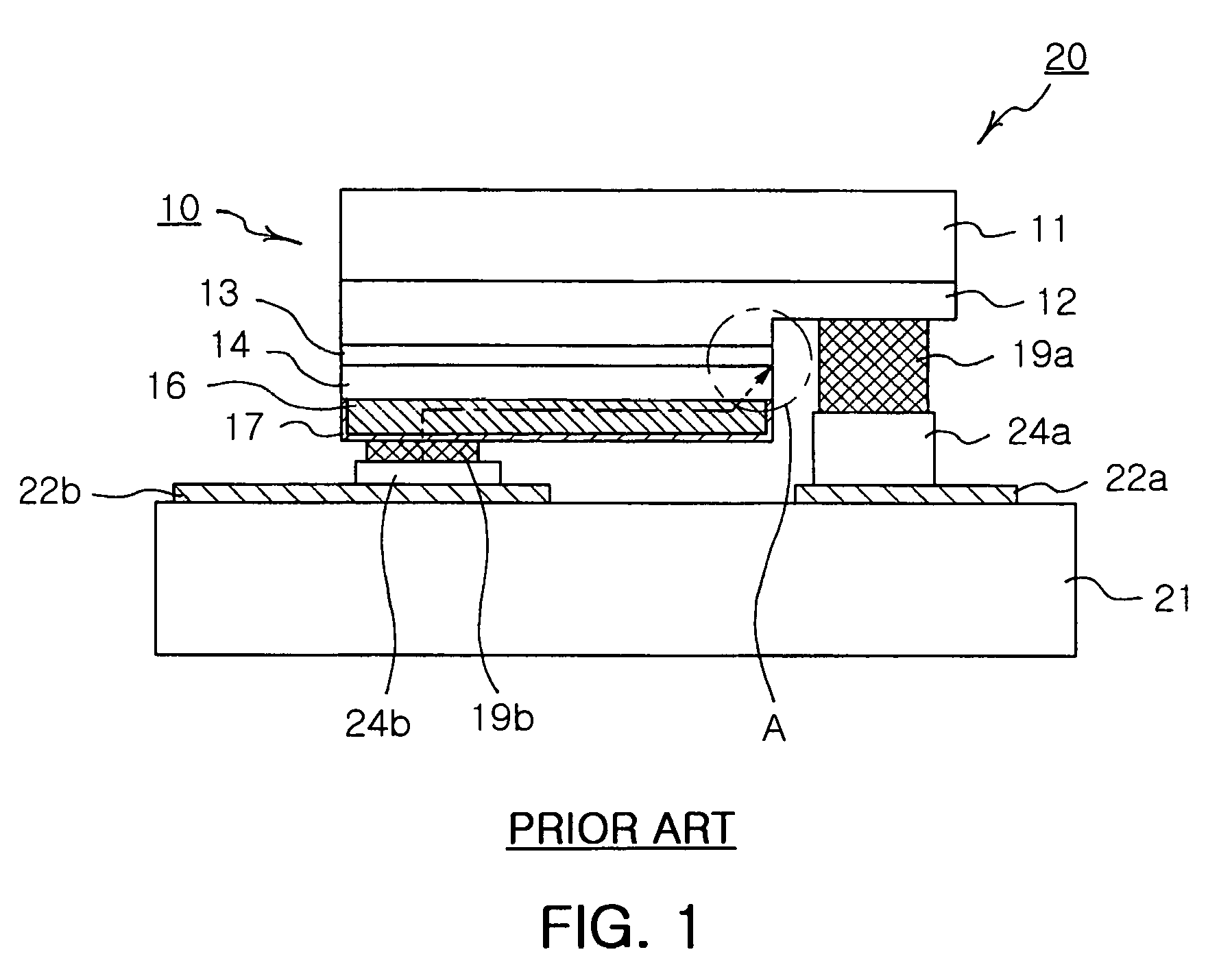
a light-emitting diode and nitride technology, applied in the direction of semiconductor devices, basic electric elements, electrical appliances, etc., can solve the problems of limited substrate used to grow such a nitride semiconductor material, metal, such as ag or al, the ohmic contact layer b>16/b> is very sensitive to heat, so as to improve current diffusion effect and reflexibility, improve the structure of the p side electrod

Inactive Publication Date: 2006-02-16
SAMSUNG ELECTRO MECHANICS CO LTD
View PDF3 Cites 99 Cited by
  • Summary
  • Abstract
  • Description
  • Claims
  • Application Information

AI Technical Summary

Benefits of technology

[0014] Therefore, the present invention has been made in view of the above problems, and it is an object of the present invention to provide a nitride semiconductor light emitting diode having an improved p-side electrode structure, thereby improving current diffusion effects and reflexibility.
[0023] In a specific embodiment of the present invention, the step of forming the mesh-type DBR reflecting layer is carried out at a temperature of 500° C. to 700° C. to prevent occurrence of cracks.

Problems solved by technology

A substrate used to grow such a nitride semiconductor material is limited to a sapphire substrate because of lattice matching.
However, the metal, such as Ag or Al, forming the ohmic contact layer 16 is very sensitive to heat.

Method used


Image

  • Nitride semiconductor light emitting diode and method of manufacturing the same
  • Nitride semiconductor light emitting diode and method of manufacturing the same
  • Nitride semiconductor light emitting diode and method of manufacturing the same

Examples


Embodiment Construction

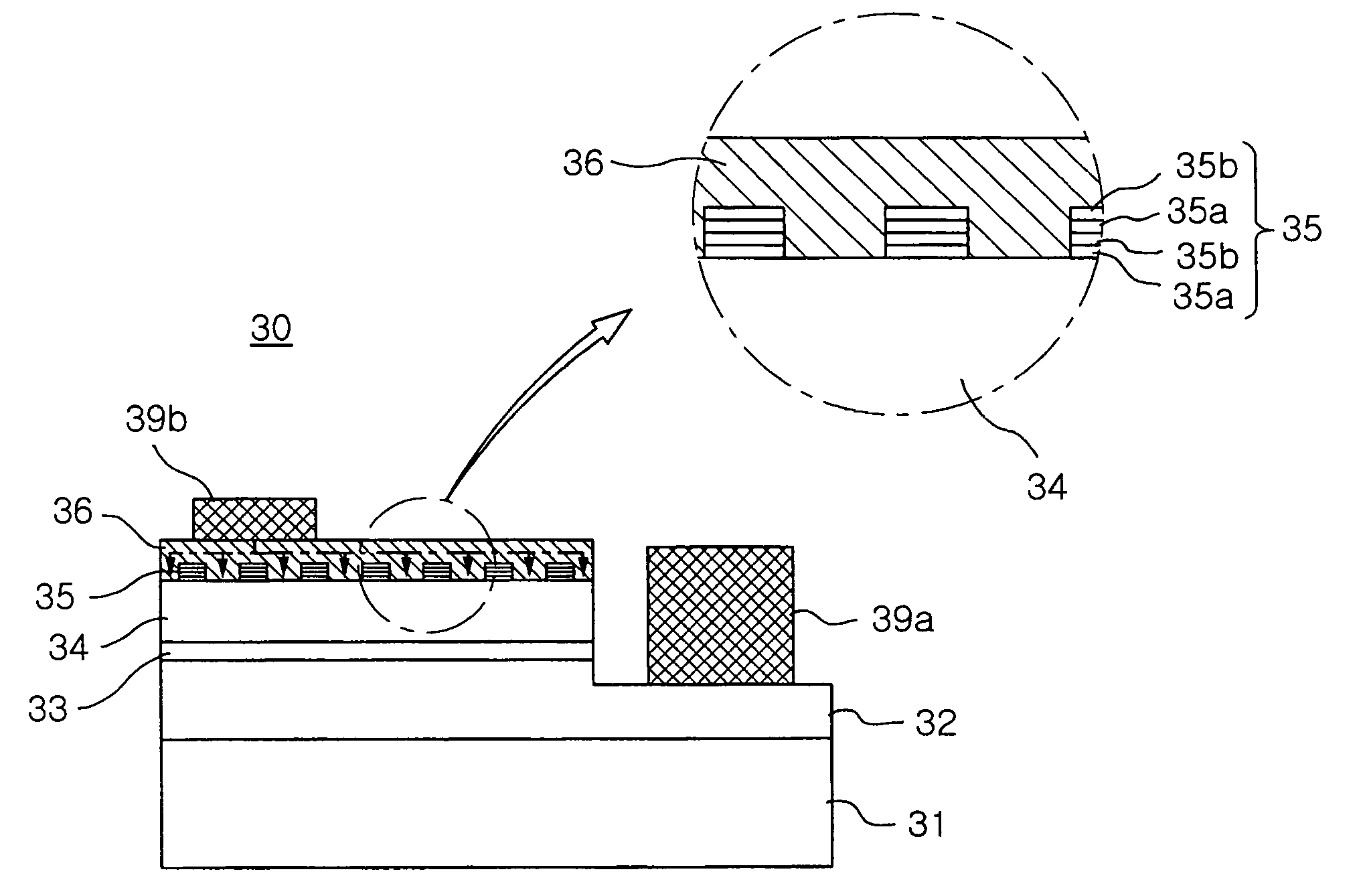
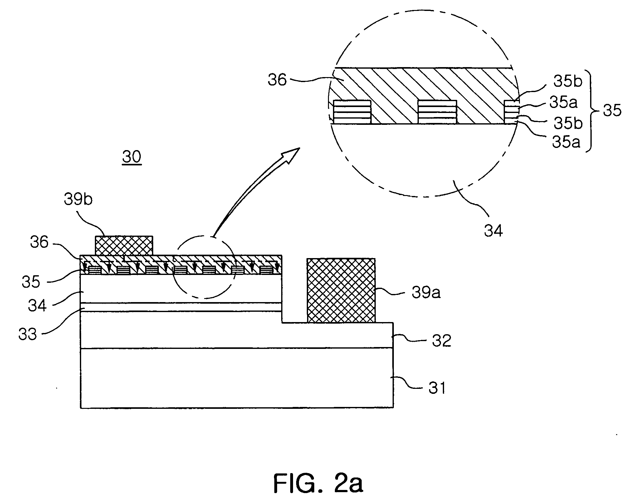
[0030] A detailed description of components of a nitride semiconductor light emitting diode according to the present invention will be given hereinafter.

[0031] P-Type and N-Type Nitride Semiconductor Layers

[0032] The p-type and n-type nitride semiconductor layers are single crystals each having the following formula: AlXInyGa(1-X-y)N (where, 0≦x≦1, 0≦y≦1, and (0≦x+y≦1), and are grown by means of Metal Organic Chemical Vapor Deposition (MOCVD), Molecular Beam Epitaxy (MBE), or Hydride Vapor Phase Epitaxy (HVPE). The typical nitride semiconductor layers include GaN, AlGaN, and GaInN.

[0033] The P-type nitride semiconductor layer may contain impurities, such as Mg, Zn, and Be. The n-type nitride semiconductor layer may contain impurities, such as Si, Ge, Se, Te, and C. Between the substrate and the nitride semiconductor layer is usually disposed a buffer layer for lattice matching. The common buffer layer may be a low-temperature core growth layer, such as AlN or GaN.

[0034] Active L...


PUM


Abstract

The present invention provides a flip chip-type nitride semiconductor light emitting diode. The nitride semiconductor light emitting diode comprises a light transmittance substrate, an n-type nitride semiconductor layer, an active layer, a p-type nitride semiconductor layer and a mesh-type DBR reflecting layer. The mesh-type DBR reflecting layer has a plurality of open regions. The mesh-type DBR reflecting layer is composed of first and second nitride layers having different Al content. The first and second nitride layers are alternately stacked several times to form the mesh-type DBR reflecting layer. An ohmic contact layer is formed on the mesh-type DBR reflecting layer and on the p-type nitride semiconductor layer.

Description

RELATED APPLICATION [0001] The present application is based on, and claims priority from, Korean Application No. 2004-63214, filed on Aug. 11, 2004, the disclosure of which is incorporated by reference herein in its entirety. BACKGROUND OF THE INVENTION [0002] 1. Field of the Invention [0003] The present invention relates to a nitride semiconductor light emitting diode, and more particularly to a nitride semiconductor light emitting diode that adopts a flip chip structure. Also, the present invention relates to a method of manufacturing the same. [0004] 2. Description of the Related Art [0005] Generally, a nitride semiconductor light emitting diode is a light emitting diode used to obtain light having a blue or green wavelength band. The nitride semiconductor light emitting diode is made of a nitride semiconductor material having the following formula: AlxInyGa(1-x-y)N [0006] Where, 0≦x≦1, 0≦y≦1, and 0≦x+y≦1 [0007] A substrate used to grow such a nitride semiconductor material is li...

Claims


Application Information

Patent Timeline
Patent Type & Authority Applications(United States)
IPC IPC(8): H01L33/00H01L33/10H01L33/32H01L33/62
CPCH01L33/32H01L33/46H01L33/405H01L33/387H01L2224/16225H01L2224/1403
Inventor LEE, JAE HOONKIM, IN EUNGKIM, YONG CHUNKIM, HYUN KYUNGKONG, MOON HEON
Owner SAMSUNG ELECTRO MECHANICS CO LTD
Why Eureka
Try Eureka