Semiconductor Device and Method of Manufacturing a Semiconductor Device Including Grinding Steps

a semiconductor and semiconductor technology, applied in the direction of semiconductor devices, semiconductor/solid-state device details, electrical equipment, etc., can solve the problems of a system of cracks, ridges and valleys, and a limited number of contact pads under the semiconductor chip,

Active Publication Date: 2013-02-28
INTEL CORP
View PDF5 Cites 217 Cited by
  • Summary
  • Abstract
  • Description
  • Claims
  • Application Information

AI Technical Summary

Problems solved by technology

Since standard wafer level packages are fan-in solutions, only a limited number of contact pads under the semiconductor chip is possible.
Any grinded semiconductor surface contains, however, a system of cracks, ridges and valleys.
These damages in the semiconductor material may induce cracks through the semiconductor bulk material if additional mechanical stress is applied.

Method used


Image

  • Semiconductor Device and Method of Manufacturing a Semiconductor Device Including Grinding Steps
  • Semiconductor Device and Method of Manufacturing a Semiconductor Device Including Grinding Steps
  • Semiconductor Device and Method of Manufacturing a Semiconductor Device Including Grinding Steps

Examples


Embodiment Construction

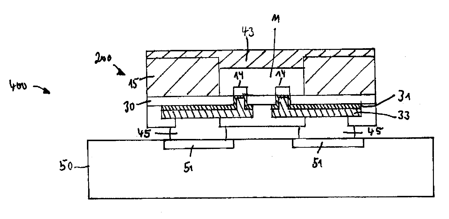
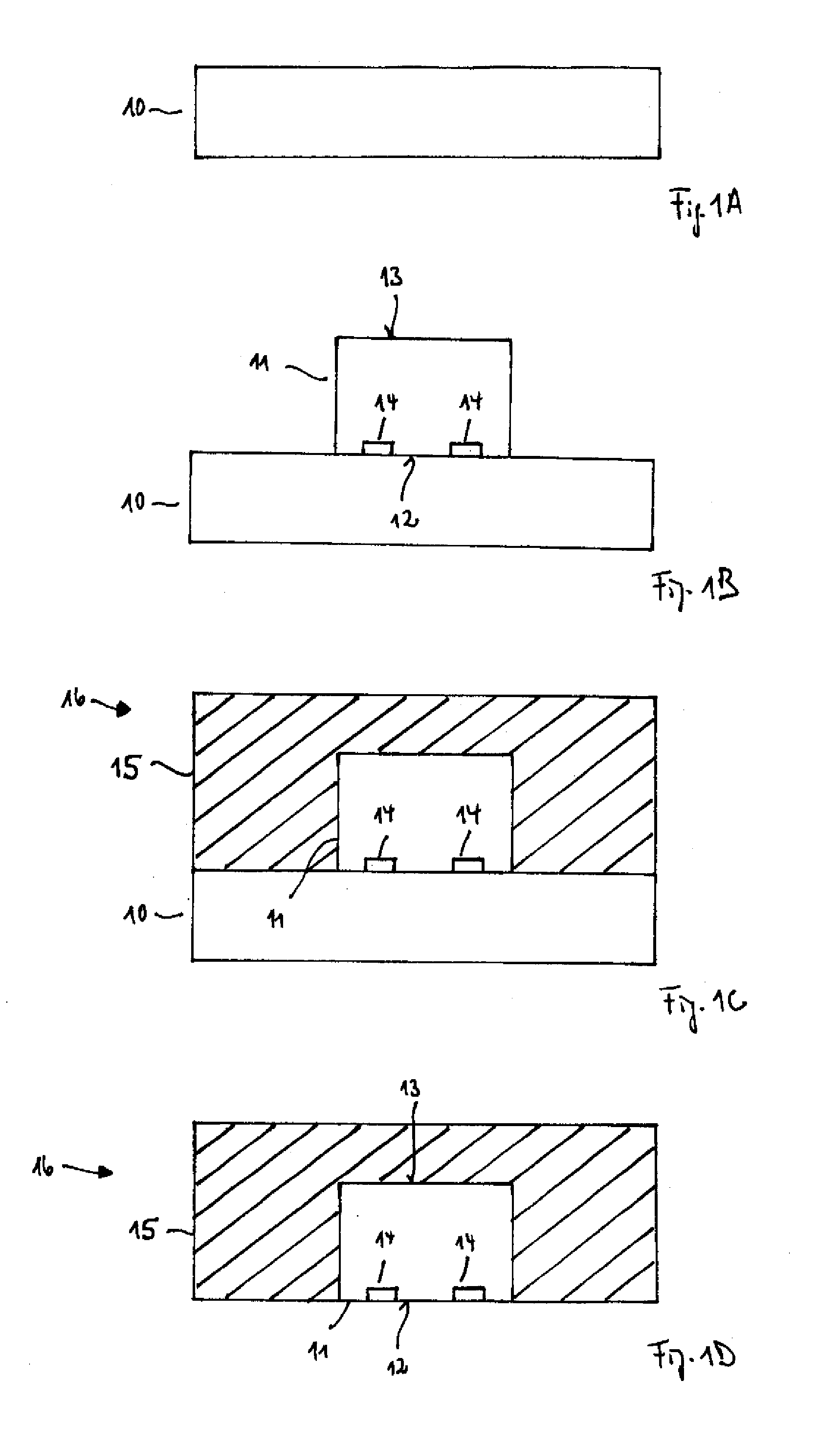
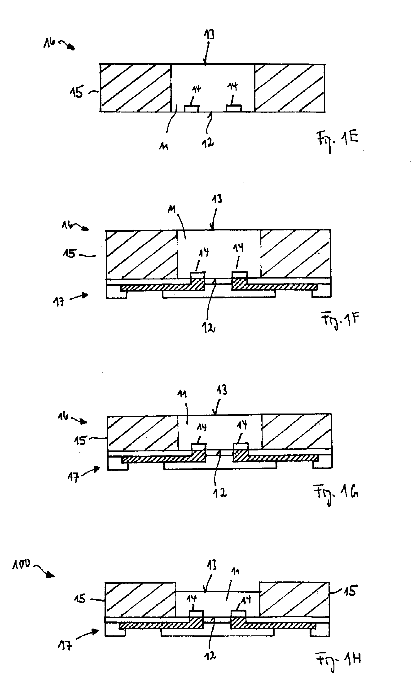
[0010]In the following detailed description, reference is made to the accompanying drawings, which form a part hereof, and in which is shown by way of illustration specific embodiments in which the invention may be practiced. In this regard, directional terminology, such as “top,”“bottom,”“front,”“back,”“leading,”“trailing,” etc., is used with reference to the orientation of the figure(s) being described. Because components of embodiments can be positioned in a number of different orientations, the directional terminology is used for purposes of illustration and is in no way limiting. It is to be understood that other embodiments may be utilized and structural or logical changes may be made without departing from the scope of the present invention. The following detailed description, therefore, is not to be taken in a limiting sense, and the scope of the present invention is defined by the appended claims.

[0011]It is to be understood that the features of the various exemplary embodi...


PUM


Abstract

A method of manufacturing a device includes providing a semiconductor chip having a first face and a second face opposite to the first face with a contact pad arranged on the first face. The semiconductor chip is placed on a carrier with the first face facing the carrier. The semiconductor chip is encapsulated with an encapsulation material. The carrier is removed and the semiconductor material is removed from the second face of the first semiconductor chip without removing encapsulation material at the same time.

Description

TECHNICAL FIELD[0001]This invention relates to a semiconductor device and a method of manufacturing a semiconductor device, wherein the method includes one or more grinding steps.BACKGROUND[0002]Wafer level packaging is gaining interest throughout the semiconductor industry due to advantages in cost and performance. When standard wafer level package technologies are used, all technology process steps are performed at the wafer level. Since standard wafer level packages are fan-in solutions, only a limited number of contact pads under the semiconductor chip is possible. Thus, for the placement of a large number of contact pads the semiconductor chip may be designed bigger or an additional material may be placed as a space holder around the die to bear the wiring that allows fan-out redistribution.[0003]Wafer level packaging usually involves grinding steps to reduce the thickness of the semiconductor die. Any grinded semiconductor surface contains, however, a system of cracks, ridges ...

Claims


Application Information

Patent Timeline
Patent Type & Authority Applications(United States)
IPC IPC(8): H01L23/48H01L21/56H01L21/50
CPCH01L23/3107H01L23/3121H01L21/561H01L21/568H01L24/19H01L24/96H01L2924/01029H01L2224/73267H01L24/20H01L2224/12105H01L2924/1461H01L21/56H01L23/3157H01L23/3185H01L2924/00H01L2924/18162H01L2924/12042H01L2224/0401H01L2223/6677H01L23/3135H01L2224/04105H01L2224/05548H01L2224/13022H01L23/28H01L23/12H01L21/02016H01L21/02013H01L21/304H01L21/311H01L21/6835H01L21/78H01L24/02H01L24/13H01L2221/68327H01L2224/0231H01L2924/2064
Inventor MEYER, THORSTENREINGRUBER, KLAUSO'SULLIVAN, DAVID
Owner INTEL CORP
Why Eureka
Try Eureka