Write transaction management within a memory interconnect

a write transaction and memory interconnect technology, applied in memory systems, electric digital data processing, instruments, etc., can solve the problems of buffer storage and address presence, and achieve the effects of low circuit overhead, high speed, and low power advantag

Active Publication Date: 2015-04-21
ARM LTD
View PDF6 Cites 0 Cited by
  • Summary
  • Abstract
  • Description
  • Claims
  • Application Information

AI Technical Summary

Benefits of technology

[0017]The technique allows the write transactions from the first transaction master and the second transaction master to take place in what would normally be regarded as the incorrect order providing data storing identification of which portions of the write line are written by the first write transaction is stored and used to prevent those portions from being overwritten by data from the cache line of data of the second write transaction. The storage requirements for the portion data are significantly less than the storage requirements for a full write transaction which would include the write line of data. In this way both increased storage requirements within the memory interconnect and disadvantageous stalling of the first transaction master may be avoided.
[0018]The serialisation circuitry serves to prevent any transaction requests sent to the shared memory until after the period when the first write transaction, any invalidation of the cache line of data and any second write transaction have indicated as completed. This ensures that the out-of-order writing of the transactions to the shared memory does not result in another master inappropriately reading the incorrect data from the shared memory at a point before the inconsistency due to the out-of-order writes has been overcome.
[0023]The first snoop request sent to the second transaction master may or may not result in a snoop response. In some embodiments, it is possible that a snoop request to return any copy of a cache line and then invalidate that cache line may be considered completed if no response is received within a given amount of time. However, in other embodiments, it may be more convenient if the write control circuitry is configured to receive a first snoop response from the second transaction master that positively indicates that the invalidation has completed. Providing for such a snoop response makes it easier to cope with systems in which the times individual transaction masters may take to process snoop requests vary due to the configuration or state of a transaction master.
[0024]The above described technique has concerned write unique transactions which write to one or more selected portions of a write line of data (typically not the full line of data). Another form of write transaction which may be encountered is a write line unique transaction which serves to write a full line of data to the shared memory. In this situation the write control circuitry may be configured to send a snoop request to the second master to trigger it to invalidate any corresponding stored cache line of data held within the local cache. The cache line of data if present need not be returned and written to the shared memory as it will be fully overwritten as a consequence of the write line unique transaction. Accordingly, the write line unique transaction may give rise to a third write transaction for writing into the shared memory the full write line without having to wait for any snoop response to the invalidation request. The serialisation circuitry is configured to stall any other transaction requests to the shared memory corresponding to the write line of data until the second snoop response and the third write transaction are indicated as completed. This avoids any intervening transaction being returned anything other than the line of data written by the write line unique transaction.
[0039]Although it is not a requirement, in some embodiments the first transaction master, the second transaction master and the memory interconnect circuitry may all be formed within a single integrated circuit. Within the same integrated circuit such high speed and low power advantages as provided by the present techniques in combination with a low circuit overhead of the memory interconnect are advantageous. The shared memory may or may not be formed on the same integrated circuit.

Problems solved by technology

However, a problem with providing local cache memories within such systems is that multiple copies of data from a given memory address are present.
While this approach has the advantage of ensuring memory consistency and correctness, it has the disadvantage of requiring buffer storage within the memory interconnect or the stalling of the transaction master which generated a stalled write request.

Method used


Image

  • Write transaction management within a memory interconnect
  • Write transaction management within a memory interconnect
  • Write transaction management within a memory interconnect

Examples


Embodiment Construction

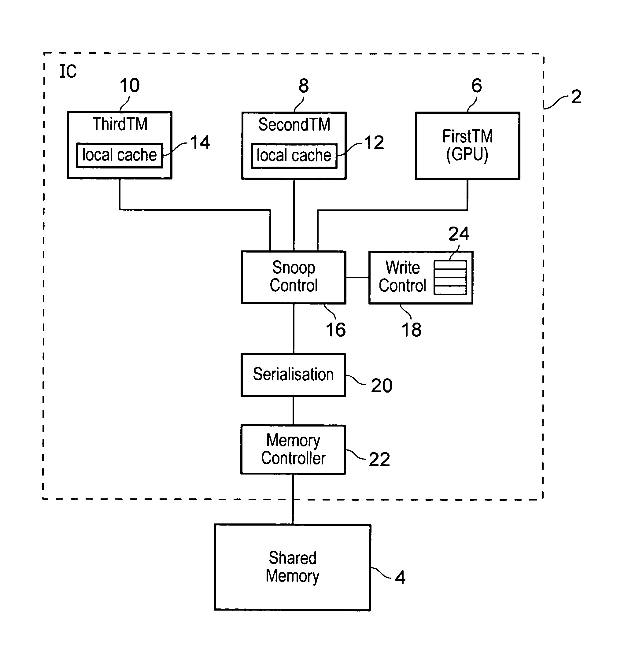
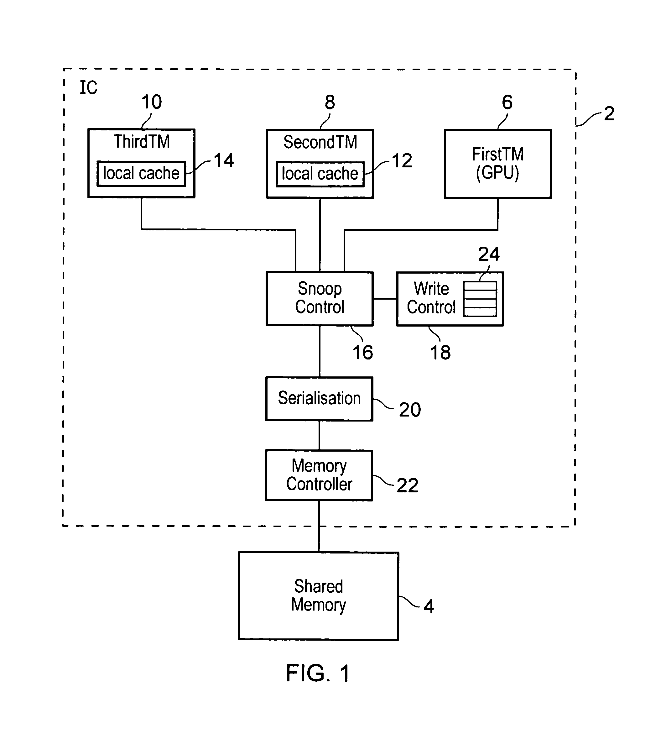
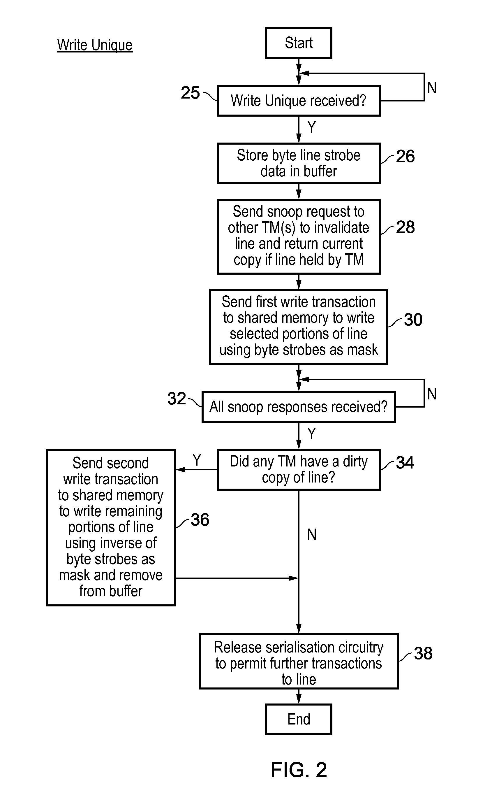
[0058]FIG. 1 schematically illustrates an integrated circuit 2 coupled to a shared memory 4. The integrated circuit 2 includes a first transaction master 6, a second transaction master 8 and a third transaction master 10. The second transaction master 8 includes a local cache memory 12 and the third transaction master 10 includes a local cache memory 14. Coherency management mechanisms within the integrated circuit include snoop control circuitry 16, write control circuitry 18 and serialisation circuitry 20. A memory controller 22 is responsible for issuing memory transactions to the shared memory 4. The write control circuitry 18 includes a buffer 24 for storing portion data formed of byte lane strobes for write unique transactions. A transaction master 6, 8, 10 may be configured to locally cache some, but not all data. Thus a master 6, 8, 10 may perform a write that is marked as not cached and this will trigger a write unique or a write line unique.

[0059]The snoop control circuitr...


PUM


Abstract

A memory interconnect between transaction masters and a shared memory. A first snoop request is sent to other transaction masters to trigger them to invalidate any local copy of that data they may hold and for them to return any cached line of data corresponding to the write line of data that is dirty. A first write transaction is sent to the shared memory. When and if any cached line of data is received from the further transaction masters, then the portion data is used to form a second write transaction which is sent to the shared memory and writes the remaining portions of the cached line of data which were not written by the first write transaction in to the shared memory. The serialization circuitry stalls any transaction requests to the write line of data until the first write transaction.

Description

BACKGROUND OF THE INVENTION[0001]1. Field of the Invention[0002]This invention relates to the field of data processing systems. More particularly, this invention relates to the management of write transactions within a memory interconnect that connects a shared memory and a plurality of transaction masters.[0003]2. Description of the Prior Art[0004]It is known to provide data processing systems that include a shared memory and a plurality of transaction masters. Such arrangements are often found within system-on-chip integrated circuits. Within such systems the different transaction masters can each generate write transactions which write data values into the address space of the shared memory. The shared memory can be accessed by more than one transaction master.[0005]It is also known within such systems that a transaction master may include a local cache memory. Providing a local cache memory within a transaction master increases the speed and efficiency of that transaction master...

Claims


Application Information

Patent Timeline
Patent Type & Authority Patents(United States)
IPC IPC(8): G06F12/00G06F12/08
CPCG06F12/0835
Inventor MACE, TIMOTHY CHARLES
Owner ARM LTD
Why Eureka
Try Eureka