Acoustic wave device

a wave device and waveguide technology, applied in the direction of impedence networks, electrical devices, etc., can solve the problems of spurious emission, deterioration of passband characteristics, and insufficient suppression of spurious emission caused, so as to achieve superior passband characteristics and suppress spurious emission

Active Publication Date: 2015-05-19
SKYWORKS PANASONIC FILTER SOLUTIONS JAPAN
View PDF5 Cites 17 Cited by
  • Summary
  • Abstract
  • Description
  • Claims
  • Application Information

AI Technical Summary

Benefits of technology

[0007]The acoustic wave device suppresses spurious emission and has superior passband characteristics.

Problems solved by technology

In this acoustic wave device, however, spurious emission is produced since, for instance, a spurious emission is caused by a higher-order transverse mode signal and other spurious emission is caused by an unwanted wave signal other than the Rayleigh wave of the main acoustic wave, deteriorating a passband characteristic of a filter.
This acoustic wave device suppresses the higher-order transverse mode spurious, but does not sufficiently suppress spurious emission caused by the unwanted wave signal other than the main acoustic wave signal.

Method used


Image

  • Acoustic wave device
  • Acoustic wave device
  • Acoustic wave device

Examples


exemplary embodiment 1

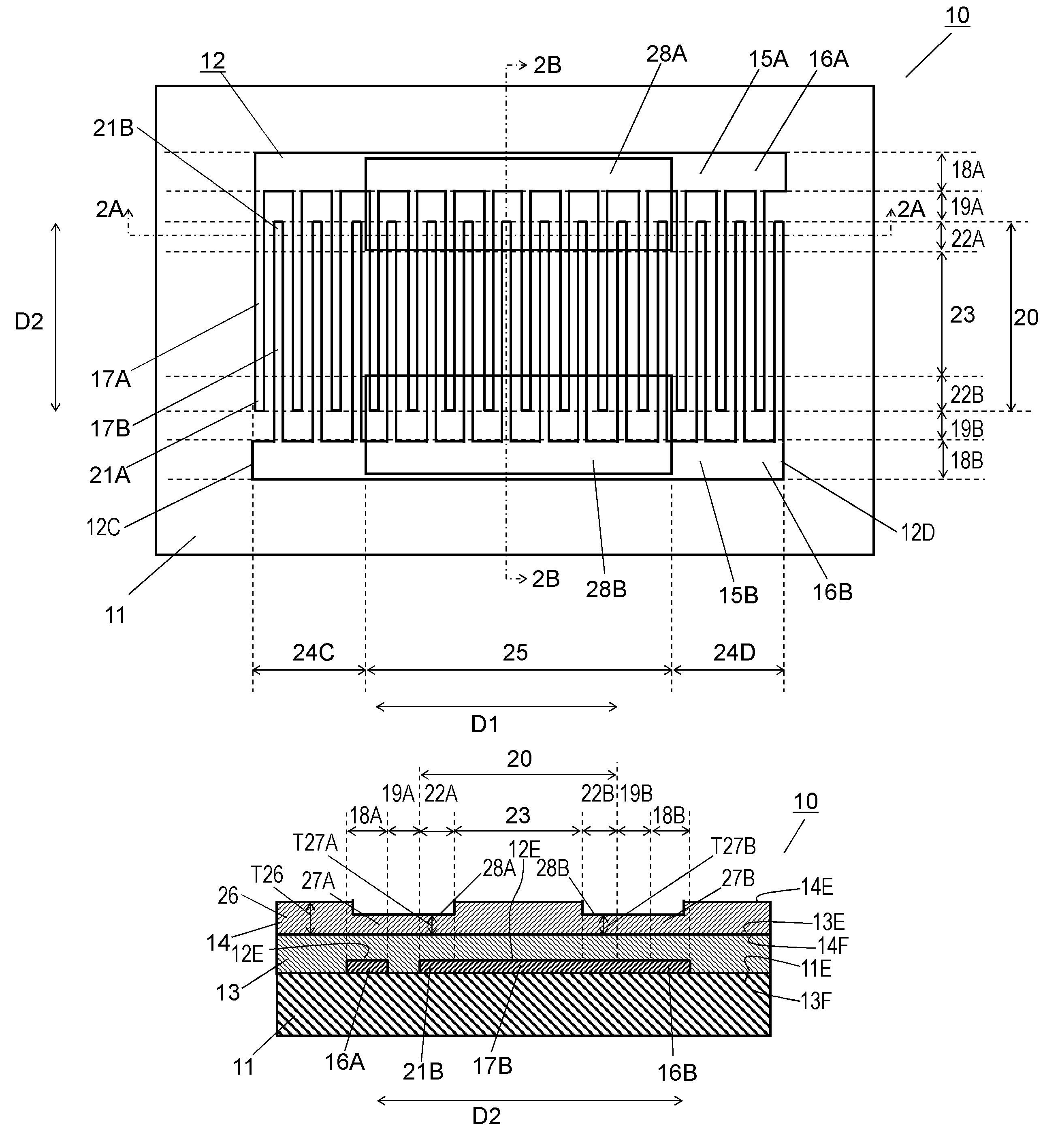
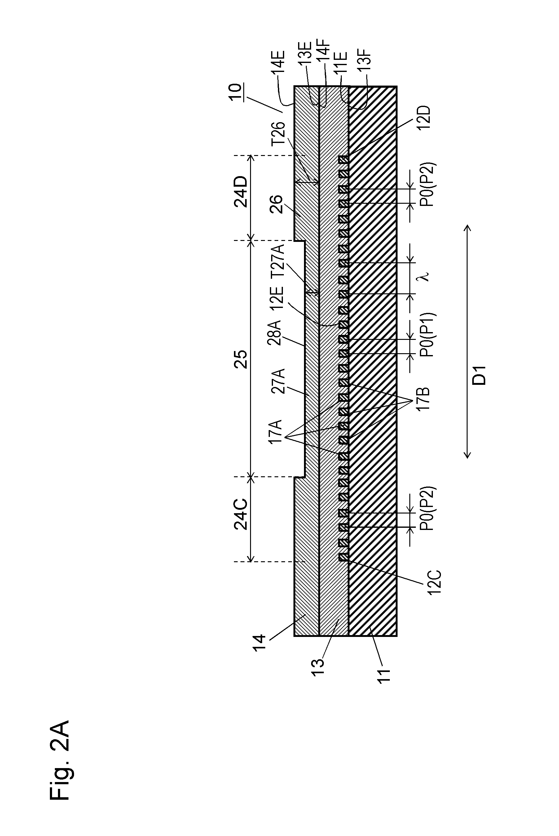
[0022]FIG. 1 is a schematic top view of acoustic wave device 10 according to Exemplary Embodiment 1 of the present invention. FIG. 2A is a cross-sectional view of acoustic wave device 10 at line 2A-2A shown in FIG. 1. FIG. 2B is a cross-sectional view of acoustic wave device 10 at line 2B-2B shown in FIG. 1.

[0023]Acoustic wave device 10 includes piezoelectric substrate 11, interdigital transducer (IDT) electrode 12 provided on upper surface 11E of piezoelectric substrate 11, dielectric film 13 provided on upper surface 12E of IDT electrode 12, and dielectric film 14 provided on upper surface 13E of dielectric film 13. Dielectric film 13 covers upper surface 11E of piezoelectric substrate 11 to cover IDT electrode 12. IDT electrode 12 includes a pair of comb electrodes 15A and 15B facing each other. Comb electrode 15A includes bus bar 16A and electrode fingers 17A extending from bus bar 16A toward comb electrode 15B in extending direction D2. Comb electrode 15B includes bus bar 16B a...

exemplary embodiment 2

[0043]FIG. 3 is a schematic depiction of a top view of acoustic wave device 40 according to Exemplary Embodiment 2 of the present invention. FIG. 4A is a schematic cross-sectional view of acoustic wave device 40 at line 4A-4A shown in FIG. 3. FIG. 4B is a schematic cross-sectional view of acoustic wave device 40 at line 4B-4B shown in FIG. 3.

[0044]In FIGS. 3, 4A and 4B, components identical to those of acoustic wave device 10 according to Embodiment 1 shown in FIGS. 1, 2A and 2B are denoted by the same reference numerals.

[0045]Acoustic wave device 40 according to Embodiment 2 is a one-terminal-pair resonator further including reflectors 29C and 29D provided at ends of IDT electrode 12 opposite to each other in propagation direction D1. Thus, IDT electrode 12 is provided between reflectors 29C and 29D in propagation direction D1.

[0046]Reflectors 29C and 29D reflect the main acoustic wave to confine the main acoustic wave in acoustic wave device 40. Reflectors 29C and 29D are made of ...

exemplary embodiment 3

[0048]FIG. 5 is a top view of acoustic wave device 50 according to Exemplary Embodiment 3 of the present invention. FIG. 6A is a cross-sectional view of acoustic wave device 50 at line 6A-6A shown in FIG. 5. FIG. 6B is a cross-sectional view of acoustic wave device 50 at line 6B-6B shown in FIG. 5. FIG. 7 is a top view of a comparative example, acoustic wave device 60. FIG. 8A is a cross-sectional view of acoustic wave device 60 at line 8A-8A shown in FIG. 7. FIG. 8B is a cross-sectional view of acoustic wave device 60 at line 8B-8B shown in FIG. 7. In FIGS. 5, 6A, 6B, 7, 8A and 8B, components identical to those of acoustic wave device 40 according to Embodiment 2 shown in FIGS. 3, 4A and 4B are denoted by the same reference numerals. Acoustic wave devices 50 and 60 are longitudinally-coupled acoustic wave filters in which IDT electrodes 12 are arranged between reflector 29C and 29D in propagation direction D1.

[0049]Each of acoustic wave devices 50 and 60 includes piezoelectric subs...


PUM


Abstract

An acoustic wave device includes a piezoelectric substrate, an interdigital transducer (IDT) electrode provided on an upper surface of the piezoelectric substrate, a first dielectric film covering the upper surface of the piezoelectric substrate to cover the IDT electrode, and a second dielectric film covering an upper surface of the first dielectric film. The second dielectric film includes a thin portion positioned in a tip region of electrode fingers of the IDT electrode and a thick portion which is positioned in a middle region of the IDT electrode and is thicker than the thin portion. The acoustic wave device suppresses spurious emission and has superior passband characteristics.

Description

TECHNICAL FIELD[0001]The present invention relates to an acoustic wave device to be used for a filter and an antenna duplexer in telecommunication equipment.BACKGROUND ART[0002]An acoustic wave device employing a 42-degree rotated Y-cut lithium tantalite board is often used for a filter and an antenna duplexer of telecommunication equipment. In recent years, a high performance acoustic wave device having a preferable temperature characteristic is demanded. To realize the acoustic wave device, a silicon dioxide film is deposited on an IDT electrode on a lithium niobate piezoelectric substrate to improve the temperature characteristic. Particularly, an acoustic wave device using lithium niobate having a cut angle to make a Rayleigh wave as a main acoustic wave is expected to realize a high resonance Q.[0003]In this acoustic wave device, however, spurious emission is produced since, for instance, a spurious emission is caused by a higher-order transverse mode signal and other spurious ...

Claims


Application Information

Patent Timeline
Patent Type & Authority Patents(United States)
IPC IPC(8): H03H9/00H03H9/25
CPCH03H9/25H03H9/02834H03H9/02858
Inventor KOMATSU, TOMOYAIWASAKI, TOMOHIRONAKAMURA, HIROYUKIYASUMI, MASAHIRONISHIMURA, KAZUNORI
Owner SKYWORKS PANASONIC FILTER SOLUTIONS JAPAN
Why Eureka
Try Eureka