
Hybrid thermal interface material for IC packages with integrated heat spreader

a heat spreader and thermal interface technology, applied in the direction of electrical equipment, semiconductor devices, semiconductor/solid-state device details, etc., can solve the problems of physical damage to the die, warpage and co-planarity of the package, and the detachment of some solder bumps, etc., to improve the mechanical strength/rigidity of the package

Active Publication Date: 2015-05-26
AVAGO TECH INT SALES PTE LTD
View PDF43 Cites 23 Cited by
  • Summary
  • Abstract
  • Description
  • Claims
  • Application Information

AI Technical Summary

Benefits of technology

The patent describes methods and systems for using different thermal interface materials to transfer heat from dies to heat spreaders and increase the mechanical strength of flip chip packages. The technical effect is better heat transfer and a stronger, more rigid package.

Problems solved by technology

Typically IC packages are asymmetrical (in the direction perpendicular to the plane of the substrate), and are mechanically unbalanced.
This asymmetry, along with the different materials used in the packaging (e.g., an organic package substrate, which has a different coefficient of thermal expansion (CTE) than the IC die), cause both mechanical and thermal stresses, which in turn lead to package warpage and co-planarity issues.
Package warp can place stress on the solder joints of the die, leading to detachment of some of the solder bumps and / or physical damage to the die.
Current adhesive materials tend to be effective at heat transfer or at warp prevention, but are not highly effective at both.

Method used


Image

  • Hybrid thermal interface material for IC packages with integrated heat spreader
  • Hybrid thermal interface material for IC packages with integrated heat spreader
  • Hybrid thermal interface material for IC packages with integrated heat spreader

Examples


example embodiments

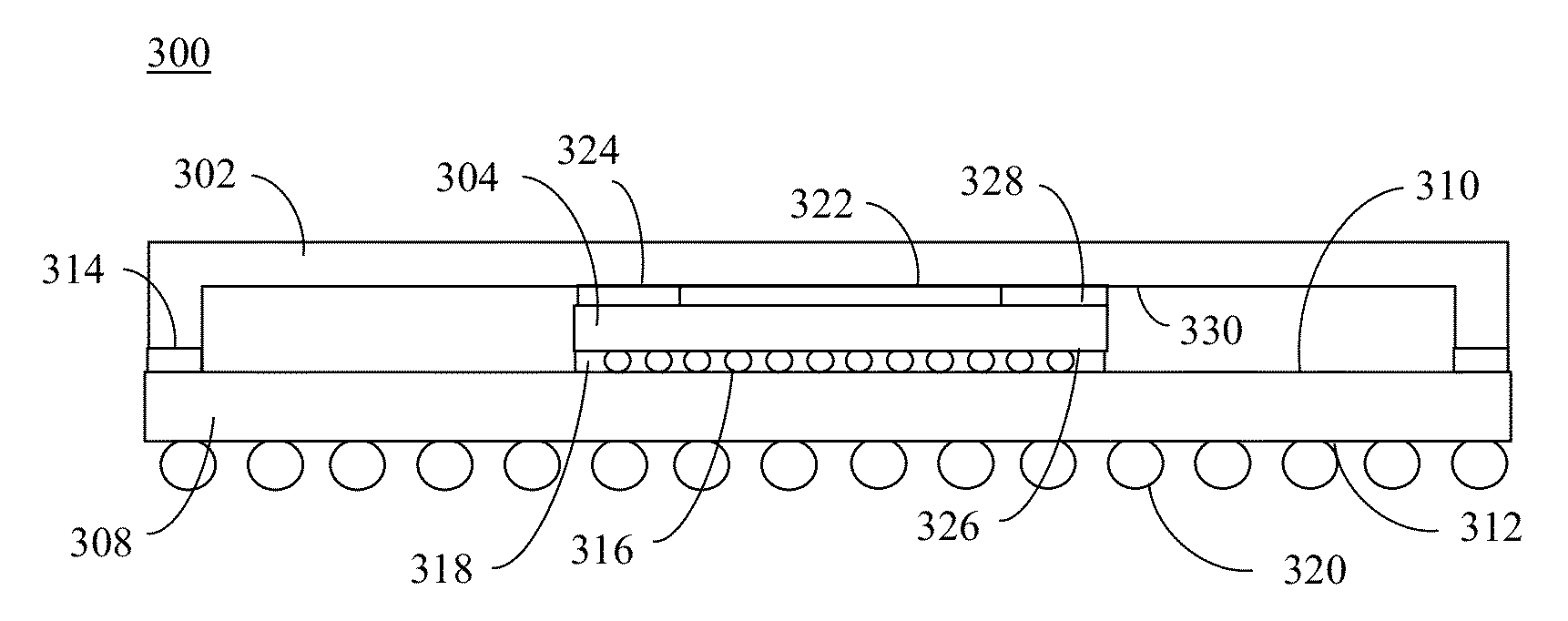
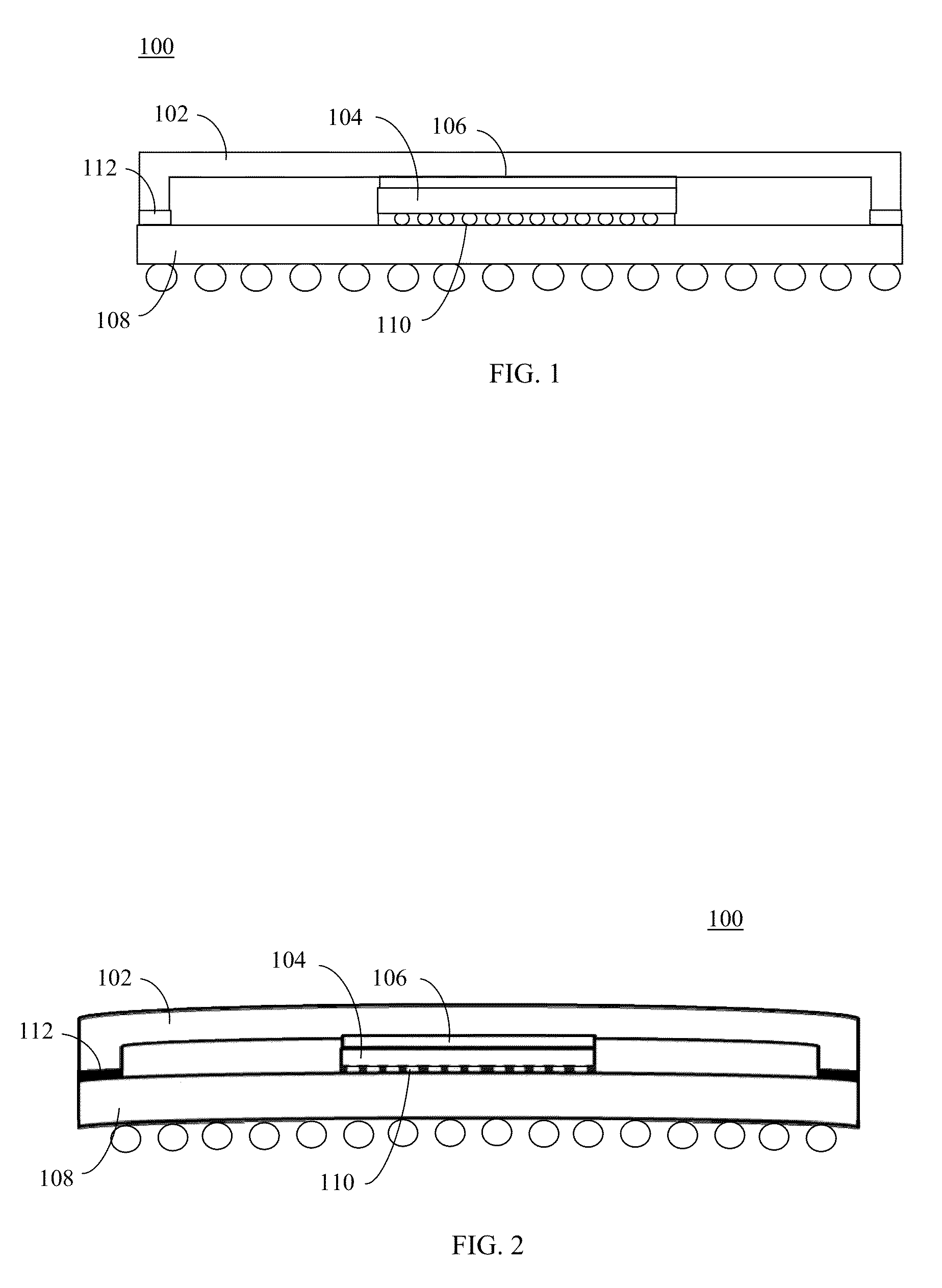
[0024]A “flip chip package” is a type of ball grid array (BGA) package that packages one or more integrated circuit dies. In a flip chip package, solder bumps are formed on the signal pads / terminals of a die, and the die is inverted (“flipped”) and attached to the substrate of the package by reflowing the solder bumps so that they attach to corresponding pads on the surface of the substrate. This inverted orientation of the die on the substrate is referred to as a “flip chip” orientation.

[0025]FIG. 1 shows a cross-sectional side view of an example flip chip package 100. As shown in FIG. 1, flip chip package 100 includes a heat spreader lid 102, an integrated circuit die / chip 104, an adhesive 106, a substrate 108, a plurality of solder bumps / balls 110, and an adhesive 112. As shown in FIG. 1, die 104 is mounted to substrate 108 by solder bumps / balls 110. Heat spreader lid 102 is mounted to substrate 108 over die 104. Adhesive 112 attaches a rim of a heat spreader lid 102 to substrate...


PUM

PropertyMeasurementUnit
thickaaaaaaaaaa
thermal resistanceaaaaaaaaaa
mechanical rigidityaaaaaaaaaa

Abstract

Flip chip packages are described that include two or more thermal interface materials (TIMs). A die is mounted to a substrate by solder bumps. A first TIM is applied to the die, and has a first thermal resistance. A second TIM is applied to the die and / or the substrate, and has a second thermal resistance that is greater than the first thermal resistance. An open end of a heat spreader lid is mounted to the substrate such that the die is positioned in an enclosure formed by the heat spreader lid and substrate. The first TIM and the second TIM are each in contact with an inner surface of the heat spreader lid. A ring-shaped stiffener may surround the die and be connected between the substrate and heat spreader lid by the second TIM.

Description

BACKGROUND[0001]1. Field of the Invention[0002]The present invention relates to integrated circuit packaging technology.[0003]2. Background Art[0004]Integrated circuit (IC) chips or dies from semiconductor wafers are typically interfaced with other circuits using a package that can be attached to a printed circuit board (PCB). One such type of IC package is a ball grid array (BGA) package. BGA packages provide for smaller footprints than many other package solutions available today. A BGA package includes a die attached to substrate of the package, and an array of solder ball pads located on a bottom external surface of the package substrate. Solder balls are attached to the solder ball pads. The solder balls are reflowed to attach the package to the PCB.[0005]In some BGA packages, signals of the die are interfaced with electrical features (e.g., bond fingers) of the substrate using wire bonds. In such a BGA package, wire bonds are connected between signal pads / terminals of the die ...

Claims


Application Information

Patent Timeline
Patent Type & Authority Patents(United States)
IPC IPC(8): H01L23/34H01L21/50H01L23/16H01L23/367H01L23/42
CPCH01L23/16H01L23/42H01L2224/16225H01L2224/32225H01L2224/73204H01L2224/73253H01L2924/15311H01L2924/16152H01L23/3675H01L2924/00H01L24/33H01L2224/29013H01L2224/29014H01L2224/29076H01L2224/3303H01L2224/33051H01L2224/33505H01L2924/3511H01L21/52H01L23/562
Inventor SAEIDI, SEYED MAHDIZHAO, SAM ZIQUN
Owner AVAGO TECH INT SALES PTE LTD
Features
  • Generate Ideas
  • Intellectual Property
  • Life Sciences
  • Materials
  • Tech Scout
  • Unparalleled Data Quality
  • Higher Quality Content
  • 60% Fewer Hallucinations
Learn More