Liquid crystal display device and method of manufacturing the same

a technology of liquid crystal display and liquid crystal, which is applied in the direction of instruments, non-linear optics, optics, etc., can solve the problems of non-uniformity of cell gap between the lower and upper substrates, and luminance also deterioration, so as to prevent luminance deterioration

Inactive Publication Date: 2015-10-27
LG DISPLAY CO LTD
View PDF7 Cites 0 Cited by
  • Summary
  • Abstract
  • Description
  • Claims
  • Application Information

AI Technical Summary

Benefits of technology

[0020]An aspect of embodiments of the present invention is directed to provide an LCD device and a method of manufacturing the same, which enables to manufacture various structures of LCD device owing to a polymer wall formed by a UV irradiation onto an upper surface of an upper substrate, and also prevents luminance deterioration owing to the polymer wall formed in a region corresponding to a gate line or data line.

Problems solved by technology

However, when curving or bending the flexible LCD device, it may have a problem related with non-uniformity in cell gap between the lower and upper substrates.
Because the polymer wall 30 is formed in the pixel region for displaying an image, light transmittance of the LCD device is lowered, and thus luminance is also deteriorated.

Method used


Image

  • Liquid crystal display device and method of manufacturing the same
  • Liquid crystal display device and method of manufacturing the same
  • Liquid crystal display device and method of manufacturing the same

Examples


first embodiment

[0047]As shown in FIG. 2A, on an upper substrate 100 of an LCD device according to the present invention, there are a light-shielding layer 110, and a color filter layer 120 interspersed within the light-shielding layer 110.

[0048]The light-shielding layer 110 prevents light from leaking in other regions except a pixel region for displaying an image. The light-shielding layer 110 may include a first light-shielding pattern 112, a second light-shielding pattern 114, and a third light-shielding pattern 116.

[0049]The first light-shielding pattern 112 is formed in the circumference of the upper substrate 100. That is, the first light-shielding pattern 112 is formed at the four sides of the upper substrate 100, on which an image is not displayed.

[0050]The second light-shielding pattern 114 and third light-shielding pattern 116 are formed inside the first light-shielding pattern 112. That is, the second light-shielding pattern 114 and third light-shielding pattern 116 are formed in the cen...

second embodiment

[0080]According to the present invention, as shown in FIG. 3A, a light-shielding layer 110 is formed on an upper substrate 100, and a color filter layer 120 is formed in the gaps of the light-shielding layers 110.

[0081]The light-shielding layer 110 may include a first light-shielding pattern 112, a second light-shielding pattern 114, and a third light-shielding pattern 116.

[0082]The second light-shielding pattern 114 is not provided with a light transparent part, and the third light-shielding pattern 116 is provided with a light transparent part 116a. Thus, when the upper surface of the upper substrate 100 is irradiated with UV light, UV light penetrates through the light transparent part 116a included in the third light-shielding pattern 116.

[0083]Eventually, as shown in FIG. 3B, a polymer wall 300 in the LCD device according to the second embodiment of the present invention comprises a second wall pattern 320 which corresponds to the light transparent part 116a included in the thi...

third embodiment

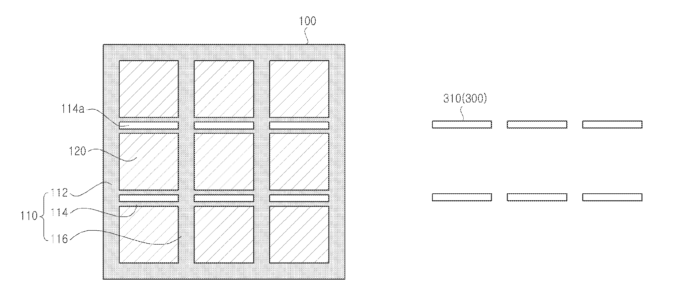
[0085]According to the present invention, as shown in FIG. 4A, a light-shielding layer 110 is formed on an upper substrate 100, and a color filter layer 120 is formed between each of the light-shielding layers 110.

[0086]The light-shielding layer 110 may include a first light-shielding pattern 112, a second light-shielding pattern 114, and a third light-shielding pattern 116.

[0087]The second light-shielding pattern 114 is provided with a light transparent part 114a, and the third light-shielding pattern 116 is not provided with a light transparent part. Thus, when the upper surface of the upper substrate 100 is irradiated with UV light, UV light penetrates through the light transparent part 114a included in the second light-shielding pattern 114.

[0088]Eventually, as shown in FIG. 4B, a polymer wall 300 in the LCD device according to the third embodiment of the present invention comprises a first wall pattern 310 which corresponds to the light transparent part 114a included in the sec...


PUM

PropertyMeasurementUnit
flexibleaaaaaaaaaa
light transparentaaaaaaaaaa
transparentaaaaaaaaaa

Abstract

Disclosed are a flexible liquid crystal display (LCD) device and a method of manufacturing the same. The flexible LCD device comprises a first flexible substrate and a second flexible substrate. A layer is disposed on the first flexible substrate and first pixel control lines are disposed on the second flexible substrate. The LCD device also includes polymer walls disposed between the first flexible substrate and the second flexible substrate that maintain a cell gap between the first flexible substrate and the second flexible substrate. The polymer walls are substantially aligned with the first pixel control lines and light transparent gaps in the layer disposed on the first flexible substrate.

Description

CROSS REFERENCE TO RELATED APPLICATIONS[0001]This application claims the benefit of the Korean Patent Application No. 10-2012-0117161 filed on Oct. 22, 2012, which is hereby incorporated by reference in its entirety.BACKGROUND[0002]1. Field of the Disclosure[0003]The present invention relates to a liquid crystal display (LCD) device, and more particularly, to a LCD device including a polymer wall for maintaining a cell gap.[0004]2. Discussion of the Related Art[0005]Owing to advantages such as good portability and low power consumption by low operating voltage, a liquid crystal display (LCD) device is widely used in various fields of notebook computer, monitor, spacecraft, aircraft, and etc.[0006]The LCD device includes a lower substrate, an upper substrate, and a liquid crystal layer formed between the lower and upper substrates.[0007]Recently, there is an increasing interest in flexible LCD device based on a flexible plastic substrate. The flexible LCD device is a rollable or wind...

Claims


Application Information

Patent Timeline
Patent Type & Authority Patents(United States)
IPC IPC(8): G02F1/1333G02F1/1335
CPCG02F1/133305G02F1/133377G02F1/133512G02F1/1335G02F1/1339
Inventor KIM, DONG GUKCHAE, GEE SUNGSHIN, DONGCHEONJANG, WON BONGLEE, JOONG HAKWAK, TAE HYOUNG
Owner LG DISPLAY CO LTD
Why Eureka
Try Eureka