
Liquid crystal display

a liquid crystal display and display device technology, applied in static indicating devices, non-linear optics, instruments, etc., can solve the problems of undesirable low total luminance supported by the applied pixel voltage, undesirable driving efficiency of the display device, and difficulty in expressing a precise gray in a low gray region. achieve the effect of preventing luminance from deteriorating

Active Publication Date: 2017-02-14
SAMSUNG DISPLAY CO LTD
View PDF20 Cites 0 Cited by
  • Summary
  • Abstract
  • Description
  • Claims
  • Application Information

AI Technical Summary

Benefits of technology

The present invention relates to a liquid crystal display that can approximate front surface visibility, provide a suitable grayscale in a low gray region, maintain satisfactory luminance, and prevent voltage changes in a pixel electrode. These technical effects enhance the display's quality and performance.

Problems solved by technology

Nevertheless, the configuration with two subpixels and with different voltages applied to the two subpixels may cause undesirably high luminance of the lateral surface at a low gray as compared to the front surface, and therefore it may be difficult to express a precise gray in a low gray region.
In addition, the total luminance supported by the applied pixel voltage may be undesirably low, and therefore the driving efficiency of the display device may be undesirable.
As a result, display quality may be undesirable.

Method used


Image

  • Liquid crystal display
  • Liquid crystal display
  • Liquid crystal display

Examples


Embodiment Construction

[0060]The present invention will be described more fully hereinafter with reference to the accompanying drawings, in which embodiments of the invention are illustrated. As those skilled in the art would realize, the described embodiments may be modified in various different ways, all without departing from the spirit or scope of the present invention.

[0061]In the drawings, the thickness of layers, films, panels, regions, etc., may be exaggerated for clarity. Like reference numerals may designate like elements throughout the specification. It will be understood that when an element such as a layer, film, region, or substrate is referred to as being “on” another element, it can be directly on the other element or intervening elements may also be present. In contrast, when an element is referred to as being “directly on” another element, there are no (intended) intervening elements (except possible environmental elements, such as air) present.

[0062]Although the terms first, second, etc...


PUM

PropertyMeasurementUnit
angleaaaaaaaaaa
angleaaaaaaaaaa
voltageaaaaaaaaaa

Abstract

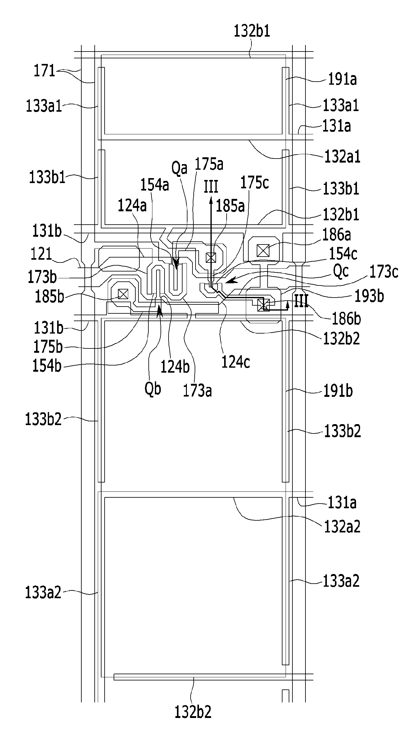
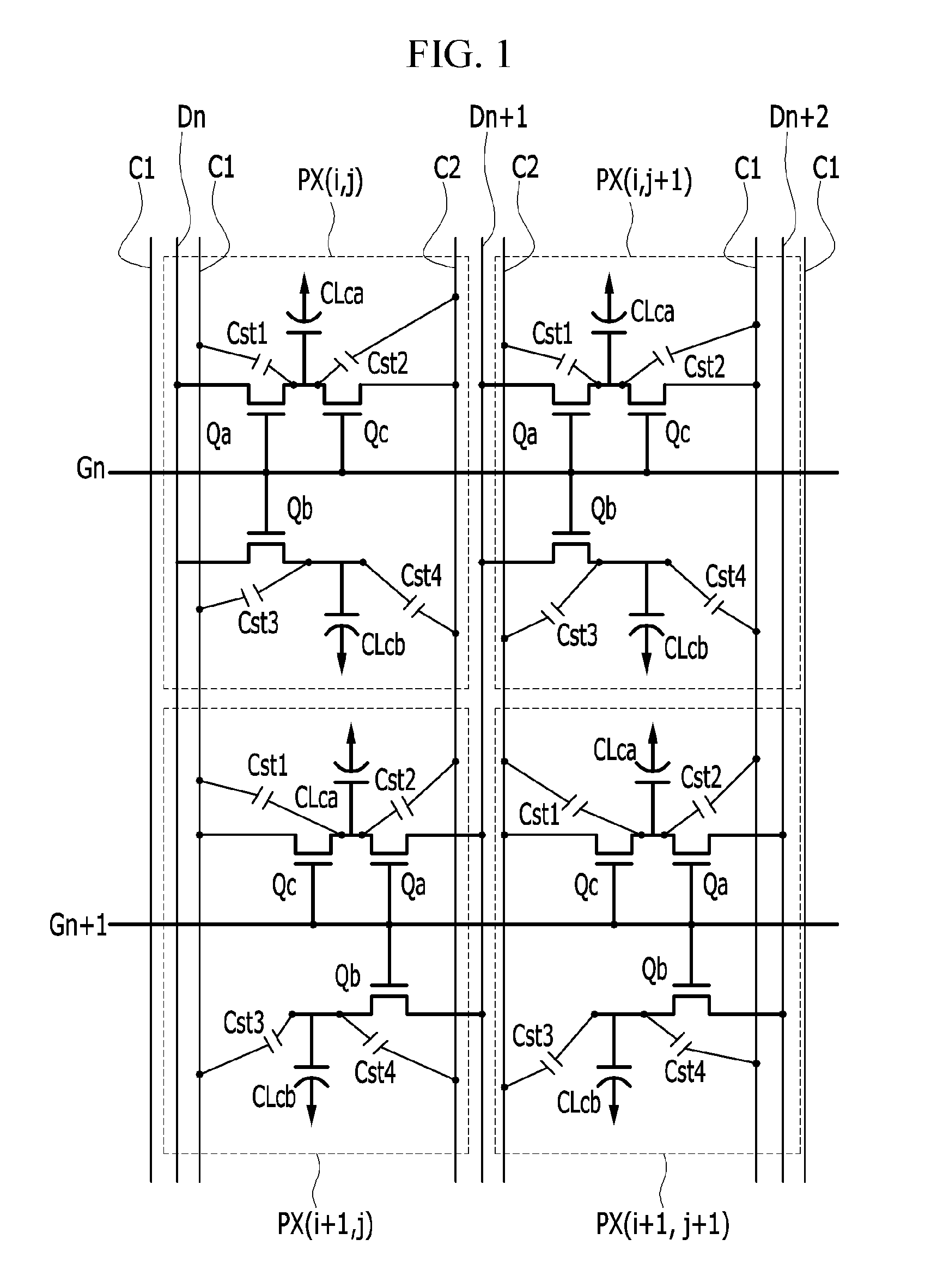
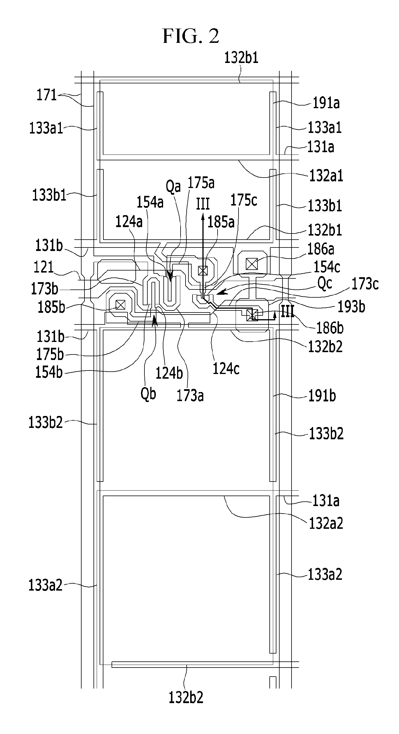
A display device includes a gate line and a data line crossing the gate line. The display device further includes a first switching element and a second switching element each connected to the gate line and the data line. The display device further includes a first sub-pixel electrode and a second sub-pixel electrode connected to the first switching element and the second switching element, respectively. The display device further includes a reference voltage line for transmitting a reference voltage, a first portion of the first reference voltage line overlapping a first edge of the first sub-pixel electrode, a second portion of the first reference voltage line overlapping a second edge of the first sub-pixel electrode opposite the first edge of the first sub-pixel electrode. The display device further includes a third switching element connected to the gate line, the first sub-pixel electrode, and the reference voltage line.

Description

CROSS-REFERENCE TO RELATED APPLICATION[0001]This application claims priority to and the benefit of Korean Patent Application No. 10-2013-0012985 filed in the Korean Intellectual Property Office on Feb. 5, 2013, the entire contents of which are incorporated herein by reference.BACKGROUND[0002](a) Technical Field[0003]The present invention relates to a liquid crystal display.[0004](b) Description of the Related Art[0005]A liquid crystal display typically includes two panels with field generating electrodes such as a pixel electrode and a common electrode and typically includes a liquid crystal layer interposed between the panels. The liquid crystal display generates an electric field in a liquid crystal layer by applying voltage to the field generating electrodes to control the orientation of liquid crystal molecules of the liquid crystal layer, thereby controlling polarization of incident light through the generated electric field and displaying desired images.[0006]A vertically alig...

Claims


Application Information

Patent Timeline
Patent Type & Authority Patents(United States)
IPC IPC(8): G02F1/1362G02F1/155G02F1/1343
CPCG02F1/13624G02F1/155G02F2001/134345G02F1/134345G02F1/133G02F1/1343G02F1/134309G02F1/136286G02F1/1368G02F2201/121G02F2201/123G09G3/2077G09G3/3607G09G3/3614G09G3/3648G09G2300/0452G09G2300/0819G09G2310/0251G09G2320/0233
Inventor JEONG, YOUN HAKKIM, SHI YULBAEK, BUM KISHIN, DONG HEELEE, HO JUNCHOI, KYONG SIK
Owner SAMSUNG DISPLAY CO LTD
Learn More