Method for manufacturing fluorescent substrate and method for manufacturing image display device

a technology of fluorescent substrate and manufacturing method, which is applied in the manufacture of electric discharge tubes/lamps, coatings, basic electric elements, etc., can solve the problems of decomposition residue of organic matter on fluorescent substrates and decrease of emission luminance, so as to inhibit the deterioration of fluorescent material luminance

Inactive Publication Date: 2010-05-27
CANON KK
View PDF4 Cites 0 Cited by
  • Summary
  • Abstract
  • Description
  • Claims
  • Application Information

AI Technical Summary

Benefits of technology

[0007]The invention provides a method inhibiting the deterioration of luminance of the fluorescent material in a process of baking the fluorescent paste.

Problems solved by technology

In this case, where the fluorescent paste is insufficiently baked, the decomposition residue of the organic matter remains on the fluorescent substrate and emission luminance decreases.

Method used


Image

  • Method for manufacturing fluorescent substrate and method for manufacturing image display device
  • Method for manufacturing fluorescent substrate and method for manufacturing image display device
  • Method for manufacturing fluorescent substrate and method for manufacturing image display device

Examples


embodiment 1

Configuration of Image Display Device

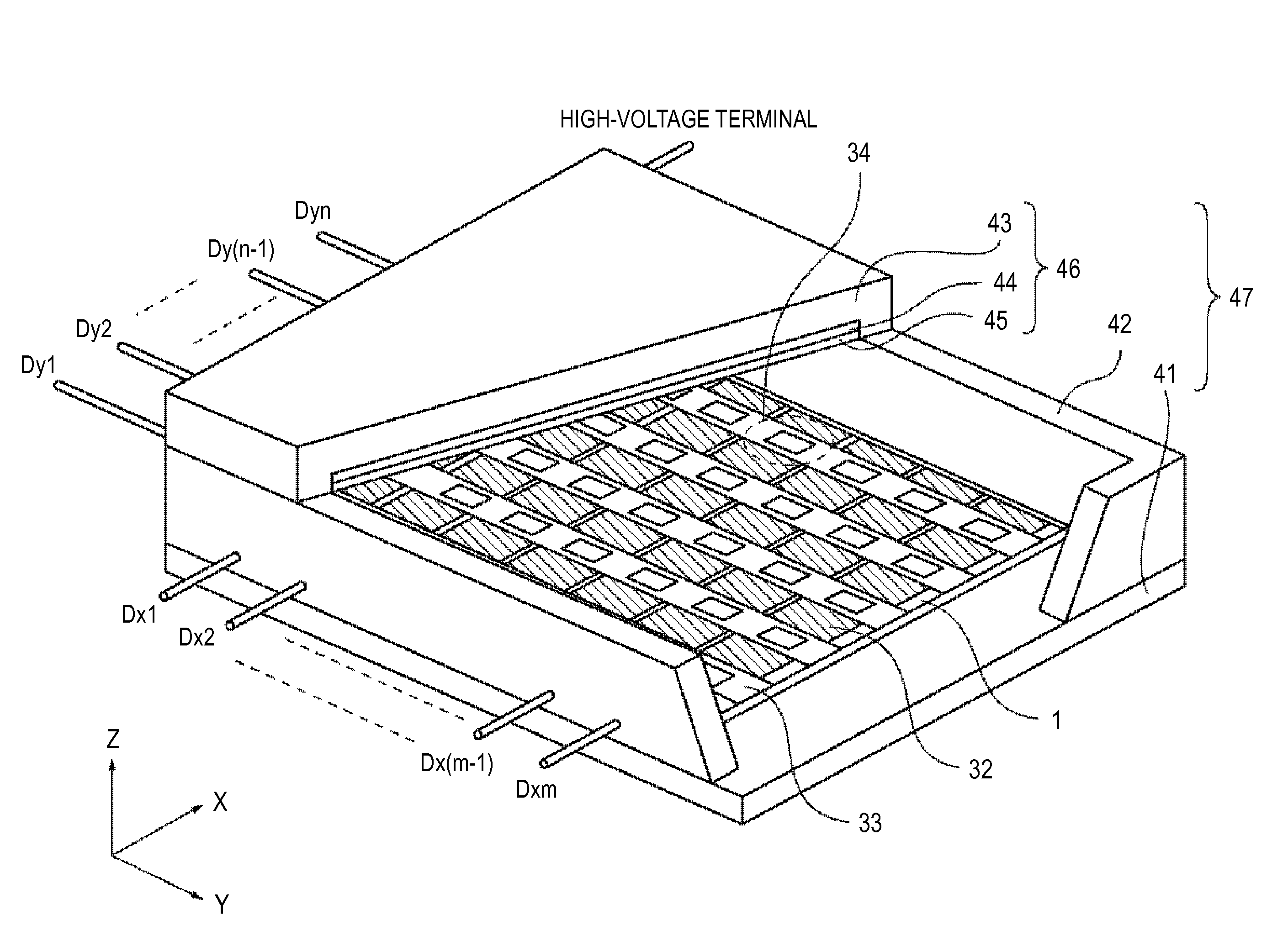
[0017]The configuration of an image display device will be explained below with reference to FIG. 1. In the present embodiment, an image display device using electron-emitting devices will be explained as the image display device.

[0018]FIG. 1 is a perspective view illustrating an example of the structure of the image display device having electron-emitting devices. Part of the structure is cut out to show the internal configuration. In the figure, the reference numeral 1 stands for a substrate, 32—a scan wiring, 33—a modulation wiring, 34—an electron-emitting device. An electron-emitting device of surface transmission type or an electron-emitting device of a spint type, MIM type, or carbon nanotube type can be used as the electron-emitting device 34. The reference numeral 41 stands for an electron source substrate fixed to the substrate 1, and 46—a fluorescent substrate in which a fluorescent material 44 and a metal back 45 as an anode electrode ...

embodiment 2

[0046]This embodiment was similar to Embodiment 1, except that the temperature profile in the baking process was different from that of Embodiment 1.

[0047]In the present embodiment, the first baking process was performed at T1=330° C. and t1=15 h and then the second baking process was performed at T2=500° C. and t2=90 min.

[0048]Where the luminance of the un-baked material (initial powder before the paste was produced) was taken as 100%, the luminance in the present embodiment was 88%.

embodiment 3

[0049]This embodiment was similar to Embodiment 1, except that the temperature profile in the baking process was different from that of Embodiment 1.

[0050]In the present embodiment, the first baking process was performed at T1=350° C. and t1=10 h and then the second baking process was performed at T2=500° C. and t2=90 min.

[0051]Where the luminance of the un-baked material (initial powder before the paste was produced) was taken as 100%, the luminance in the present embodiment was 89%.


PUM

PropertyMeasurementUnit
current voltageaaaaaaaaaa
temperatureaaaaaaaaaa
thicknessaaaaaaaaaa

Abstract

The method for manufacturing a fluorescent paste includes a process of applying a fluorescent paste including a sulfide fluorescent material and a binder resin onto a substrate, a first baking process of baking the substrate for a predetermined time at a first temperature that is equal to or lower than a temperature at which a generated amount of water has a maximum in a case where the fluorescent paste is measured by a TDP-MS method, and a second baking process of baking the substrate for a predetermined time at a second temperature that is equal to or higher than a temperature at which a generated amount of carbon dioxide has a minimum in a case where the fluorescent paste is measured by a TDP-MS method after the first baking process.

Description

BACKGROUND OF THE INVENTION[0001]1. Field of the Invention[0002]The present invention relates to a method for manufacturing a fluorescent substrate and also to a method for manufacturing an image display device having a fluorescent substrate.[0003]2. Description of the Related Art[0004]Image display devices in which an image is displayed by light emission from a fluorescent material, such as a FED (Field Emission Display) or PDP (Plasma Display Panel), are known. In the process of manufacturing a fluorescent substrate for such image display devices, a fluorescent paste is used in which fluorescent particles are dispersed in a binder resin and a solvent. Where screen printing is conducted by using the fluorescent paste and the fluorescent paste is then baked, the organic components of the binder resin are decomposed and a fluorescent substrate is formed.[0005]In this case, where the fluorescent paste is insufficiently baked, the decomposition residue of the organic matter remains on ...

Claims


Application Information

Patent Timeline
Patent Type & Authority Applications(United States)
IPC IPC(8): H01J9/24B05D5/06
CPCH01J9/221
Inventor HIGUCHI, HIROSHIMIIDA, ATSUSHISASAGURI, DAISUKESARUTA, SHOSHIROONO, TAKEO
Owner CANON KK
Why Eureka
Try Eureka