Row driving circuit for array substrate and liquid crystal display device

a technology of array substrate and driving circuit, which is applied in the field of array substrate and liquid crystal display device, can solve the problems of affecting the cost of the components rising, and the yield declining, so as to improve the stability of the output of the goa circui

Active Publication Date: 2015-12-15
TCL CHINA STAR OPTOELECTRONICS TECH CO LTD
View PDF6 Cites 4 Cited by
  • Summary
  • Abstract
  • Description
  • Claims
  • Application Information

AI Technical Summary

Benefits of technology

[0007]An object of the present invention is to provide a row driving circuit for an array substrate and a liquid crystal display device, which can avoid the threshold voltage shift of the TFT elements, so as to improve the stability of the output of the GOA circuit.
[0038]wherein a pull-up unit is connected to the high frequency clock signal input terminal and the first output terminal; the pull-up controlling unit and the pull-up unit are connected to the second output terminal for charging a signal of the first output terminal, and thus the second output terminal has a higher electric potential;
[0067]wherein a pull-up unit is connected to the high frequency clock signal input terminal and the first output terminal; the pull-up controlling unit and the pull-up unit are connected to the second output terminal for charging a signal of the first output terminal, and thus the second output terminal has a higher electric potential;
[0071]Unlike the prior art, the first thin film transistor of the GOA circuit of the present invention is controlled by the signal of a previous stage, and the signal delivered between the previous stage and the next stage of the GOA circuit is less affected by the threshold voltage shift of the TFT elements than it is in the traditional GOA circuit. Thus, the output of the GOA circuit can avoid being affected by the threshold voltage shift of the TFT elements and the stability of the output can be improved.

Problems solved by technology

However, multilayer metal traces are not suited for applying to a narrow bezel and will probably result in a short circuit in a panel, so that the yield declines and the costs of the components rise.
In practice, most of the GOA circuits have some limitations.
For example, TFT (Thin Film Transistor) elements of the GOA circuit produce a threshold voltage shift for stress resistance, thus affecting the stability of the output of the GOA circuit.

Method used


Image

  • Row driving circuit for array substrate and liquid crystal display device
  • Row driving circuit for array substrate and liquid crystal display device
  • Row driving circuit for array substrate and liquid crystal display device

Examples


Embodiment Construction

[0077]The structure and the technical means adopted by the present invention to achieve the above and other objects can best be understood by referring to the following detailed description of the preferred embodiments and the accompanying drawings. Furthermore, the directional terms described by the present invention, such as upper, lower, front, back, left, right, inner, outer, side, longitudinal / vertical, transverse / horizontal, and etc., are only directions by referring to the accompanying drawings, and thus the used directional terms are used to describe and understand the present invention, but the present invention is not limited thereto.

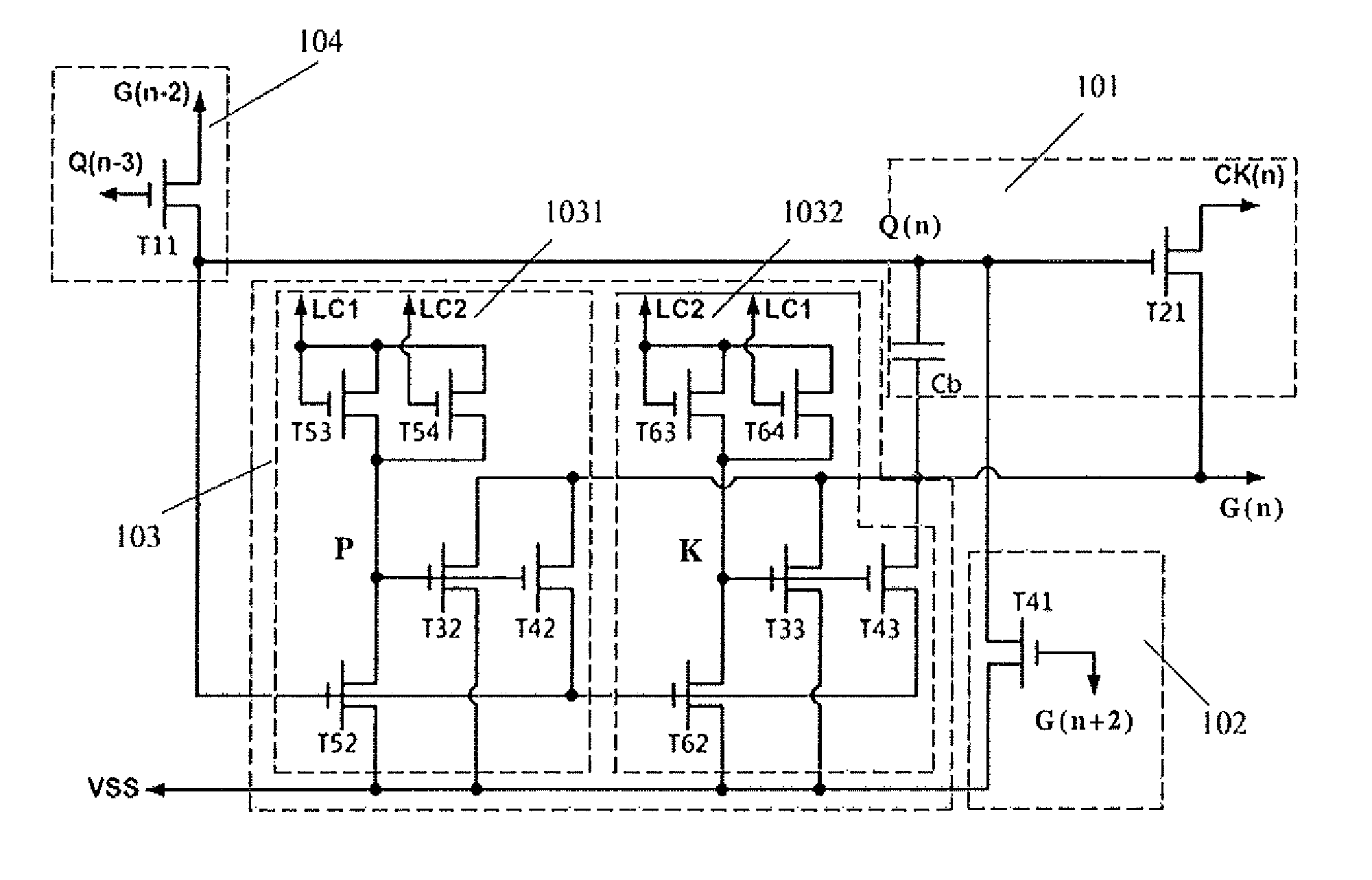
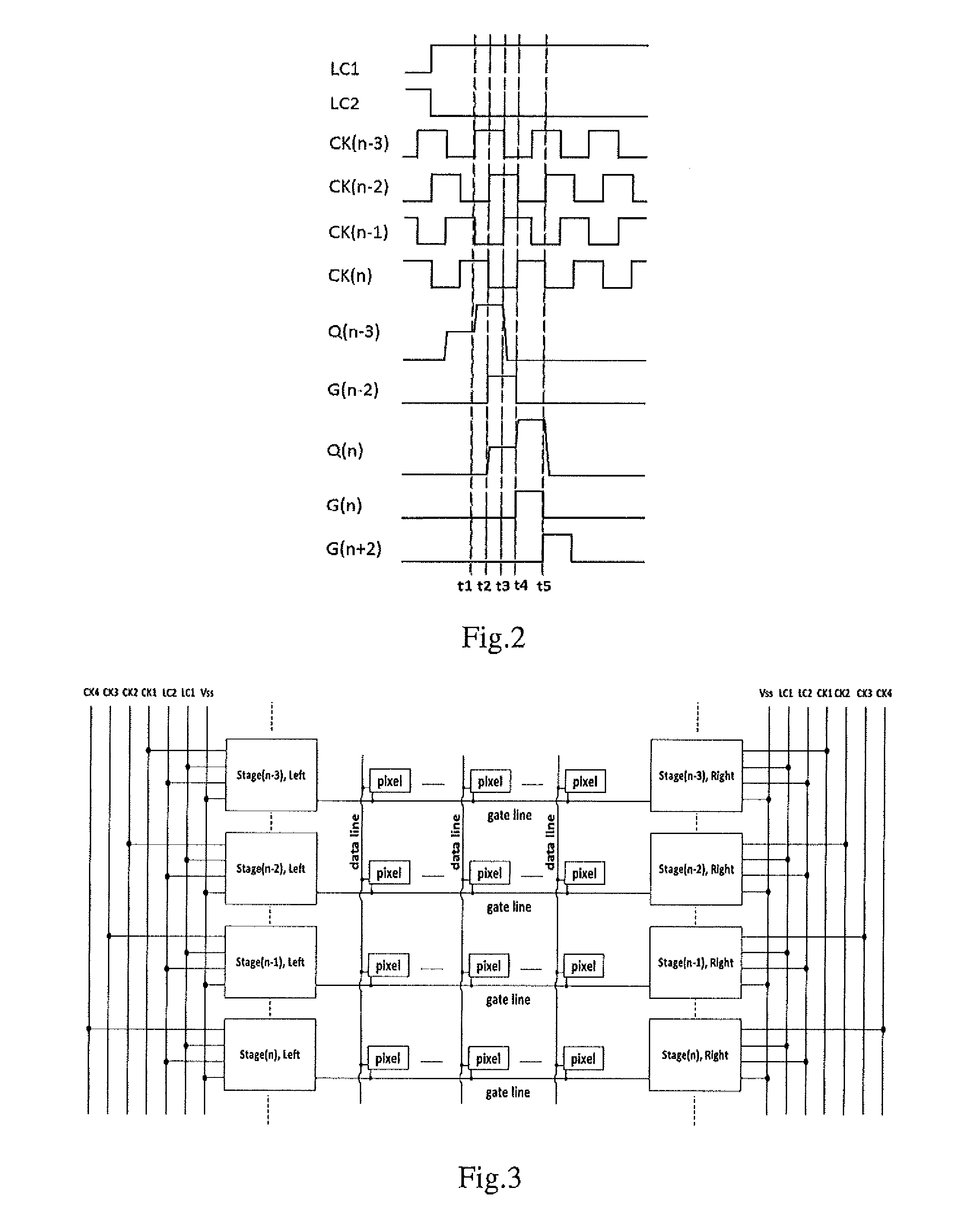
[0078]FIG. 1 is a schematic view of a structure of a row driving circuit for an array substrate according to a first embodiment of the present invention.

[0079]The row driving circuit for an array substrate comprises array substrate row driving units with multi-stage connections. An n-th stage array substrate row driving unit in the row driving...


PUM


Abstract

An n-th stage array substrate row driving unit of a row driving circuit for an array substrate is provided. The n-th stage array substrate row driving unit comprises an (n−3)-th and an (n−2)-th stage signal input terminal and a pull-up controlling unit. The pull-up controlling unit is a first thin film transistor and is connected to the (n−2)-th and a (n−3)-th stage signal input terminal. A peak voltage of the (n−3)-th stage signal input terminal is twice a peak voltage of the (n−2)-th stage signal input terminal. Thus, the threshold voltage shift of the TFT elements can be avoided, and the stability of the output can be improved.

Description

RELATED APPLICATIONS[0001]This application is a National Phase of PCT Patent Application No. PCT / CN2014 / 079928 having International filing date of Jun. 16, 2014, which claims the benefit of priority of Chinese Patent Application No. 201410226117.1 filed on May 26, 2014. The contents of the above applications are all incorporated by reference as if fully set forth herein in their entirety.FIELD OF THE INVENTION[0002]The present invention relates to the technical field of a display panel, and more particularly to a row driving circuit for an array substrate and a liquid crystal display device.BACKGROUND OF THE INVENTION[0003]In traditional display panels, a narrow bezel technology is generally utilized.[0004]In general, adopt Multilayer Metal Traces or Gate electrode driver On Array (GOA) technology is applied in traditional narrow bezels. However, multilayer metal traces are not suited for applying to a narrow bezel and will probably result in a short circuit in a panel, so that the ...

Claims


Application Information

Patent Timeline
Patent Type & Authority Patents(United States)
IPC IPC(8): G09G3/36
CPCG09G3/3648G09G3/3677G09G3/3696G09G2300/0404G09G2300/0426G09G2300/0478G09G2300/0408G09G2310/0281G09G2310/0283G09G2310/0286
Inventor YU, XIAOJIANGLEE, CHANG YEHLAI, TZU-CHIEH
Owner TCL CHINA STAR OPTOELECTRONICS TECH CO LTD
Why Eureka
Try Eureka