Method to prevent lateral epitaxial growth in semiconductor devices
- Summary
- Abstract
- Description
- Claims
- Application Information
AI Technical Summary
Benefits of technology
Problems solved by technology
Method used
Image

Examples
Example
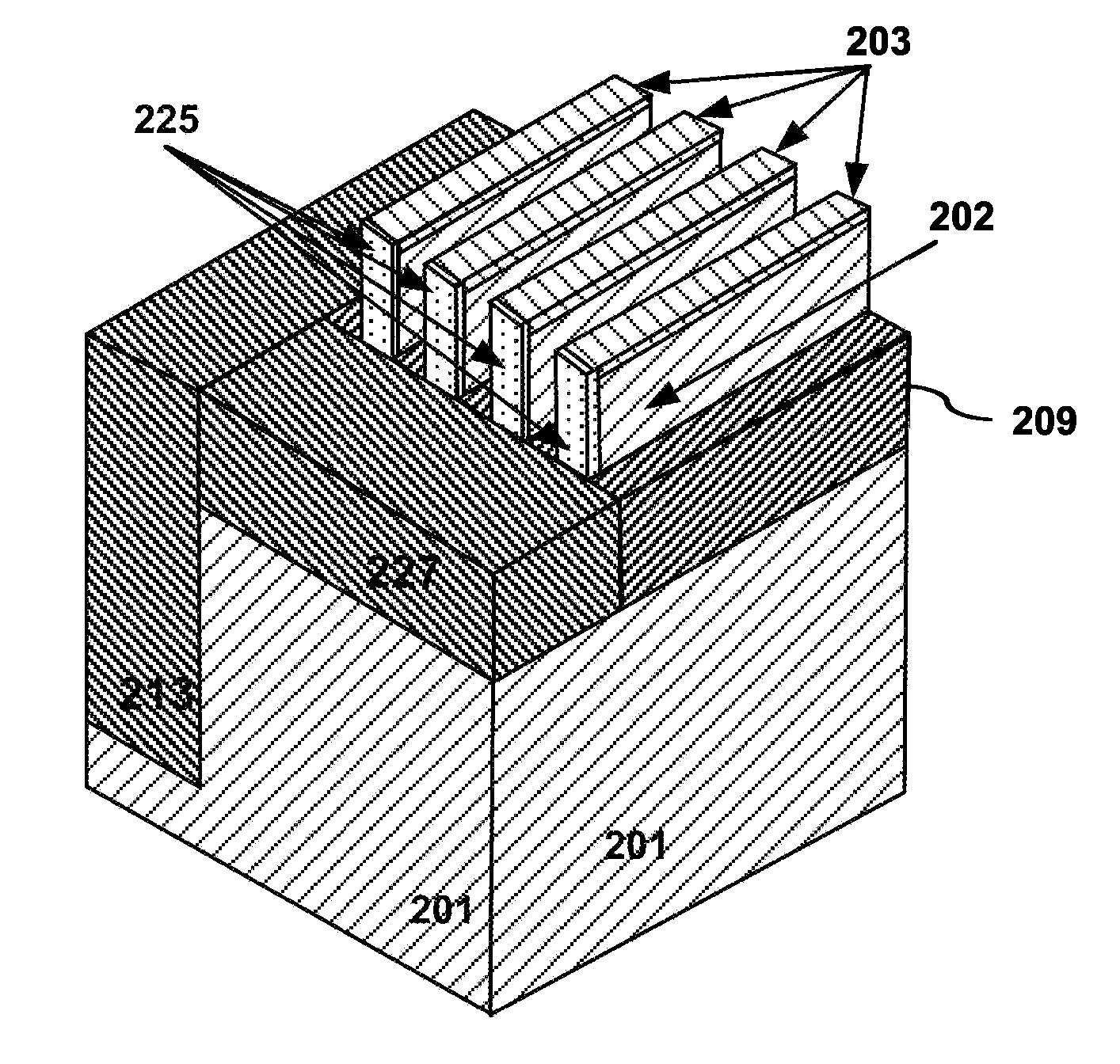
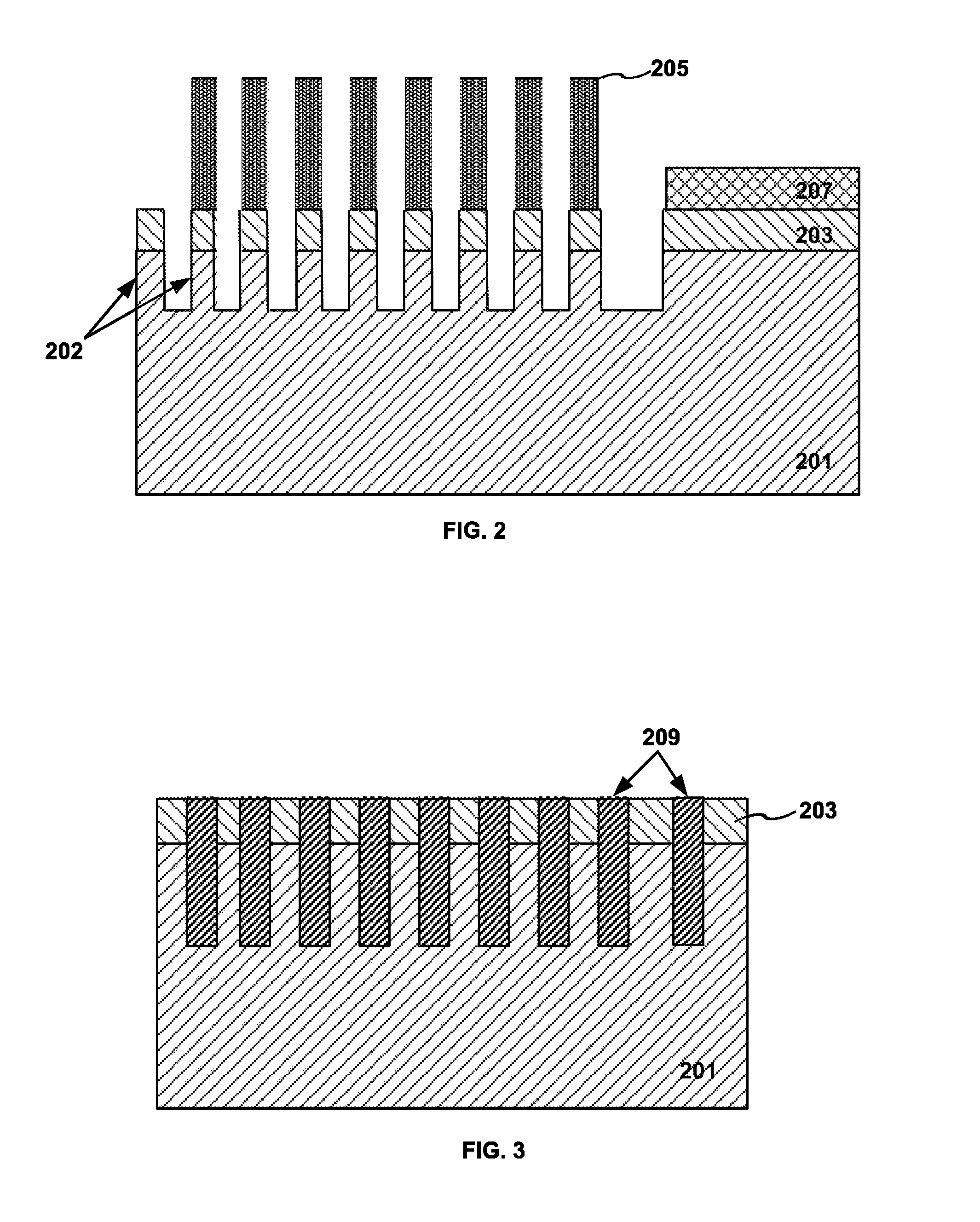
[0035]In FIG. 9A, a second embodiment of the invention is shown. FIG. 9B is a perspective drawing at the same point in the process. The processing for the second invention is similar to that shown in FIGS. 2-6 for the first invention. Then after the fins are cut, by photo lithography and etch as shown FIGS. 9A and 9B, the exposed fin ends 202 of the FinFET structure are exposed to plasma nitridation and / or high dose implantation (portrayed as arrows 233) to create an inhibitory layer which inhibits excessive epitaxial growth at the fin ends. Different embodiments of the invention will use either plasma nitridation or high dose implantation; some embodiments of the invention can use both processes in combination. A plasma nitridation process will form a SiN layer on the exposed fin tip to prevent epitaxial growth. The high dose implantation can use zirconium (Zr) or argon (Ar) ions to create a thin amorphous silicon layer at the fin end 202. Those skilled in the art will recognize th...
PUM
 Abstract
Description
Claims
Application Information
 - Generate Ideas
- Intellectual Property
- Life Sciences
- Materials
- Tech Scout
- Unparalleled Data Quality
- Higher Quality Content
- 60% Fewer Hallucinations
Browse by: Latest US Patents, China's latest patents, Technical Efficacy Thesaurus, Application Domain, Technology Topic, Popular Technical Reports.
© 2025 PatSnap. All rights reserved.Legal|Privacy policy|Modern Slavery Act Transparency Statement|Sitemap|About US| Contact US: help@patsnap.com