Circuit arrangement and method for receiving digital optical signals

a digital optical and circuit technology, applied in electromagnetic receivers, electrical equipment, electromagnetic transmission, etc., can solve the problems of inability to determine unequivocally, use of such transcoding schemes, and increase the energy consumption of the entire transmission path, so as to achieve the highest direct gigabit data rate and reduce the complexity of circuit data preparation

Active Publication Date: 2016-08-23
SILICON LINE
View PDF7 Cites 3 Cited by
  • Summary
  • Abstract
  • Description
  • Claims
  • Application Information

AI Technical Summary

Benefits of technology

[0036]This makes it possible using the present invention, to utilise certain circuit arrangements and / or certain circuit techniques to receive random input data, i.e. random digital optical data streams in a band width range from zero bit per second up to the high Gbit / s range for a minimum of circuitry and low energy consumption.
[0042]The circuit arrangement according to the present invention as well as the method according to the present invention represent a possibility of optically transmitting both DC signals and maximum-frequency data in an uncoded way over the same transmission channel. By means of the present invention it is possible to provide true opto couplers for highest direct Gigabit data rates.
[0043]The receiver part of the circuit arrangement as well as its mode of operation make it possible to receive, without errors, a randomly coded or uncoded, not DC-balanced serial bit stream of an optical data transmission path. In contrast to solutions from the state of the art the circuit arrangement according to the present invention as well as the method according to the present invention offer the possibility of processing a bit stream in a power-saving manner, for a distinctly reduced circuit complexity in data preparation.

Problems solved by technology

Apart from a data overhead being created the transcoding operation also increases energy consumption of the entire transmission path.
With very high bitrates in particular internal data preparation accounts for a considerable share in the overall energy consumption so that the use of such transcoding schemes is not always a preferred option.
But since the data stream, which initially is not pre-conditioned for optical transmission is, as a rule, DC-unbalanced, meaning that because logical “1” and logical “0” do as a rule not occur evenly distributed in the incoming data stream during the optical transmission, conventionally used extraction methods are unable to determine unequivocally that voltage level of the incoming data stream, which defines the middle between the logical “1” and the logical “0”.
DC current compensation can now be automatically regulated on the basis of the input data, but this is connected with a certain amount of necessary circuitry which delays processing of the incoming signals.

Method used


Image

  • Circuit arrangement and method for receiving digital optical signals
  • Circuit arrangement and method for receiving digital optical signals

Examples


Embodiment Construction

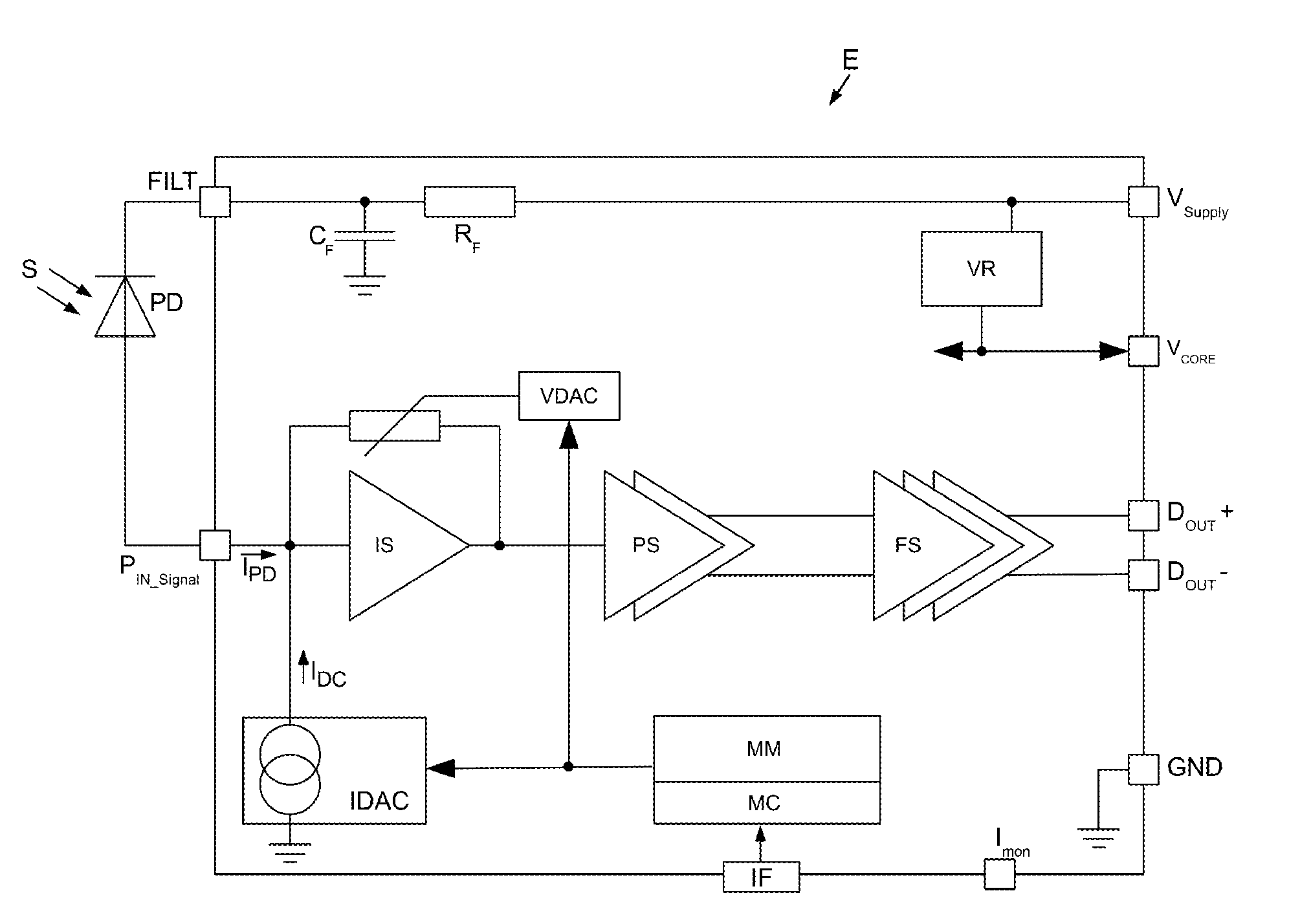
[0048]Digital optical signals S can be received by means of the circuit arrangement E according to the present invention, as shown in FIG. 1. To this end a light-receiving element in the form of a photodiode PD is arranged at the entry to circuit arrangement E upstream of a signal input port PIN-Signal.

[0049]A filter input connection FILT is arranged upstream of the photodiode PD which, via a filter member comprising[0050]a capacitor CF and[0051]an ohmic resistance RF

is associated with an externally applied supply voltage VSupply, which, for example, may vary within a range between approximately 2.5 volt and approximately 3.3 volt. The capacitor plate of the filter capacitor CF facing away from the filter resistance RF is connected with a reference potential GND, in particular earth potential or ground potential or zero potential.

[0052]For generating an additional supply voltage VCORE, which is smaller than the externally applied supply voltage VSupply, in particular lies between a...


PUM


Abstract

In order to be able to receive any digital optical signals in the bandwidth range from zero bits per second to the high Gbits / second range with as little circuit complexity as possible and to be able to process said signals with the least possible energy requirement for reprocessing, the invention proposes a circuit arrangement as well as a method for receiving digital optical signals by means of at least one light-receiving component connected upstream of at least one signal input port, particularly by means of at least one photodiode, wherein the unipolar current signal coming from the light-receiving component through the signal input port is transformed into a bipolar current signal by means of a compensation current provided by at least one current source, the value of said current being defined by means of at least one digital register.

Description

CROSS-REFERENCE TO RELATED APPLICATIONS[0001]This application is a continuation of international (WO) patent application no. PCT / DE2013 / 200015, filed 22 May 2013, which claims the priority of German (DE) patent application no. 10 2012 104 420.1, filed 22 May 2012, the contents of each being hereby incorporated herein by reference.FIELD OF THE INVENTION[0002]The present invention principally relates to the technical field of serialised optical and / or electrical signal connections; more specifically, the present invention relates to a circuit arrangement as well as to a method for receiving digital optical signals.BACKGROUND OF THE INVENTION[0003]High-bit-rate serial connections—whether electrical or optical—as a rule require that the bit stream to be transmitted is D[irect]C[urrent]-balanced or DC-balanced. Fundamental circuit parts in such a transmission path are conceptually dependent on this property of the DC-balance of the data stream in order to function.[0004]In order to conve...

Claims


Application Information

Patent Timeline
Patent Type & Authority Patents(United States)
IPC IPC(8): H04B10/69
CPCH04B10/6911H04B10/697
Inventor GROEPL, MARTINFRITSCHE, HOLGERHOELTKE, HOLGER
Owner SILICON LINE
Why Eureka
Try Eureka