Frame boundary discriminator

a boundary discriminator and frame signal technology, applied in the field of telephony digital signal transmission, can solve the problems of increasing the sensitivity of the system to clock skew, the limited capacity of related state machines to process signals in such a system, so as to achieve smooth out jitter and high tolerance of jitter

Active Publication Date: 2007-07-10
ZARLINK SEMICON LTD
View PDF9 Cites 2 Cited by
  • Summary
  • Abstract
  • Description
  • Claims
  • Application Information

AI Technical Summary

Benefits of technology

[0010]The present invention thus provide a means of establishing a periodic reference signal divided down from a higher speed periodic signal with the reference signal aligned in phase to an external reference signal of the same frequency. The phase alignment process is highly tolerant of jitter on the external reference signal, effectively eliminating all jitter within a narrow phase error band in creating the internal reference. It uses an averaging technique to create this internal reference signal with minimal circuitry.
[0011]The invention also provides a method of discriminating frame boundaries in a digital telephony, comprising the steps of generating a high speed master clock signal having a multitude of master clock pulses within a frame; receiving synchronized input frame pulses subject to jitter; comparing the timing of said synchronized input frame pulses with said master clock pulses; generating output frame pulses from said master clock pulses; and adjusting the timing of said output frame pulses to smooth out jitter in said input frame pulses.

Problems solved by technology

The capacity of related state machines to process signals in such a system is limited by the number of clock cycles available in a 125 microsecond frame.
This constraint may be reduced by increasing the frequency of the clock available to each individual circuit in the system, but the usage of higher speed clocks has the drawback of increasing the sensitivity of system to clock skew between components as well as increasing the level of electromagnetic radiation emanating from the clock tracking on the circuit board.

Method used


Image

  • Frame boundary discriminator
  • Frame boundary discriminator
  • Frame boundary discriminator

Examples


Embodiment Construction

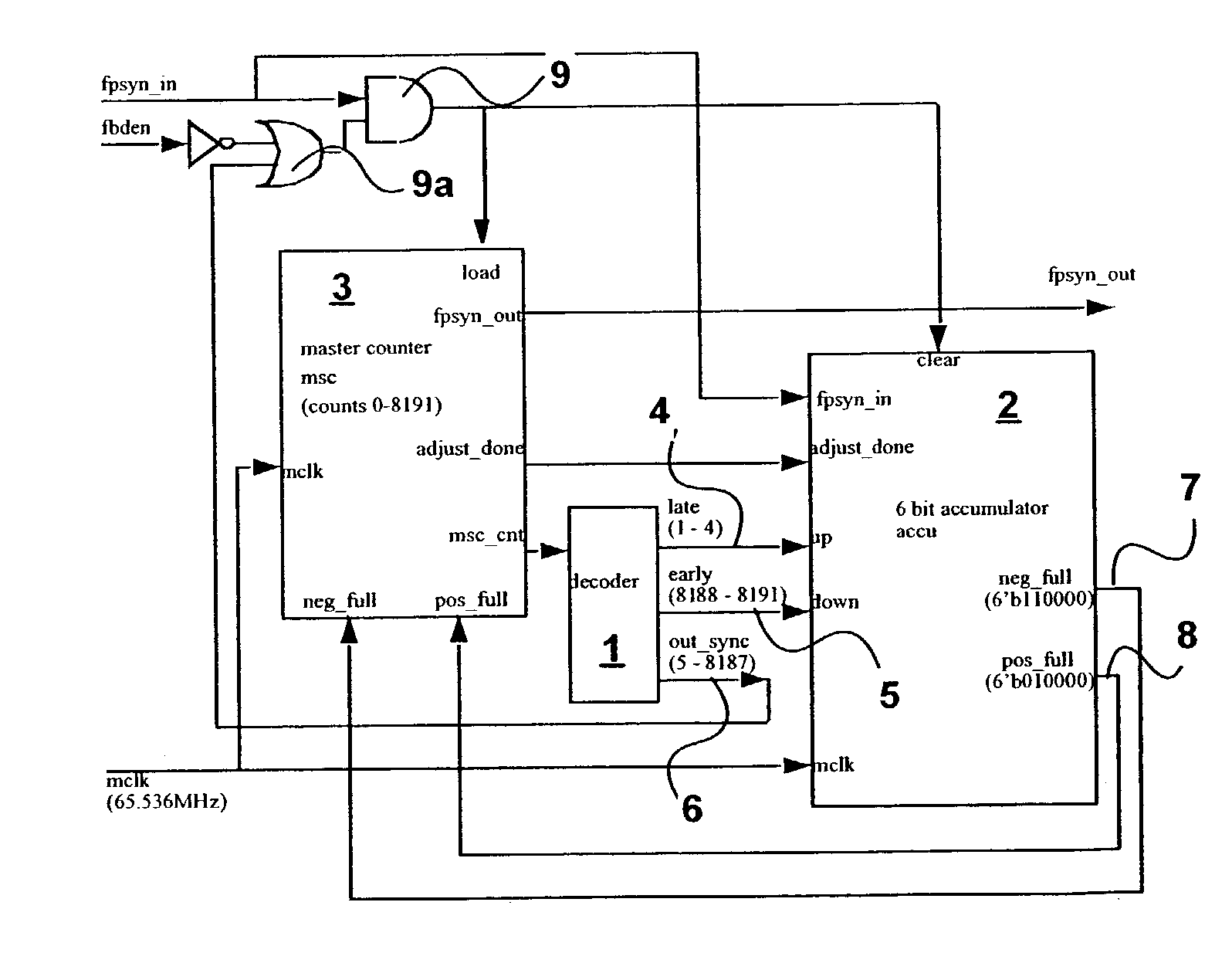
[0021]The described circuit in accordance with the invention generates an internal frame pulse which is stable even with a jittered input reference clock and input frame pulse. A higher speed master clock and a synchronized input frame pulse are required by this circuit. These are used as primary input signals.

[0022]Referring first to FIG. 6, the boundary discriminator circuit comprises three major blocks, namely a decoder 1, an accumulator 2 (accu), and a master counter 3 (msc). The counter 3 is a modulo 8191 counter that can have a count value anywhere between 0 and 8191.

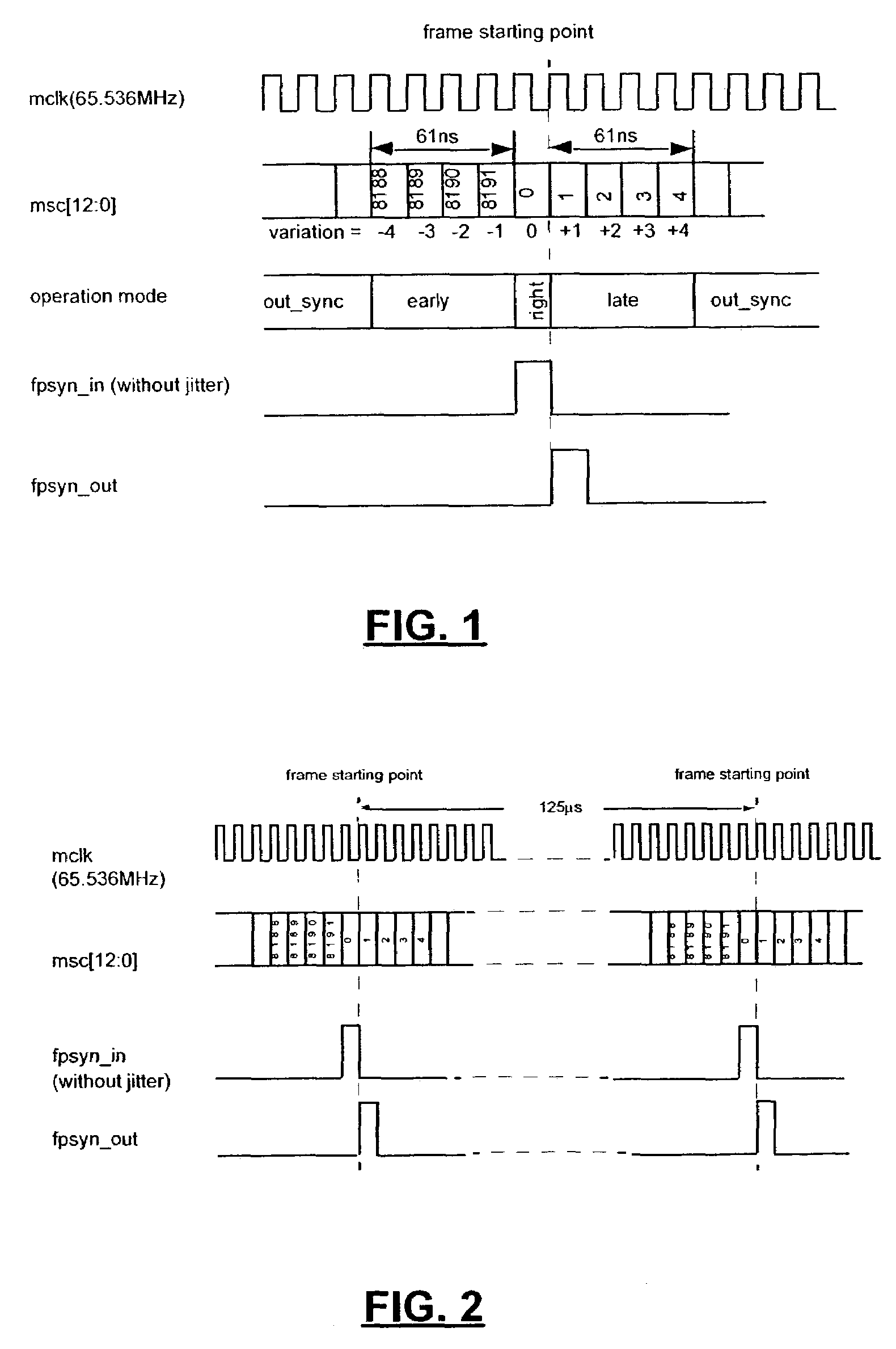
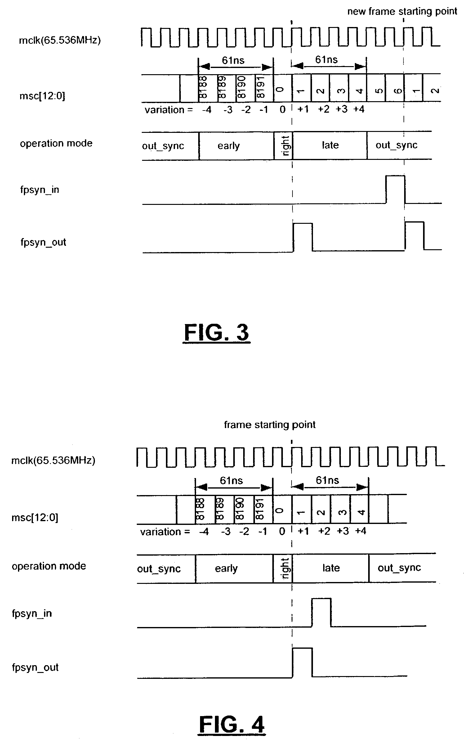
[0023]Decoder 1 decodes the count value of counter 3 and generates a late signal 4 when an input frame pulse arrives and the count value is 1-4, an early signal 5 when the count value is 8188-8191, and an out_of_sync signal 6, when the count value is from 5-8187. Signals 4 and 5 are input to the accumulator 2, which generates enables signals neg_full 7 and pos_full 8 in a manner to be described. Signal 6 is passed...


PUM


Abstract

A frame boundary discriminator has a first input for receiving a high speed master clock signal having a multitude of master clock pulses within a frame, and a second input for receiving synchronized input frame pulses subject to jitter. An output frame pulse generator controlled by the high speed master clock signal generates output frame pulses. A control circuit for compares the timing of the synchronized input frame pulses with said master clock pulses and adjusts the timing of said output frame pulses to average out jitter in the input frame pulses.

Description

BACKGROUND OF THE INVENTION[0001]1. Field of the Invention[0002]This invention relates to telephony digital signal transmission, and more particularly to a method of boundary discrimination of a frame signal which defines the starting point of data to be transmitted or received.[0003]2. Description of Related Art[0004]Digital telephone circuits carry signals within predetermined time periods known as frames delineated by an 8 KHz timing signal or clock known as a frame pulse, which establishes a frame boundary. Each frame therefore defines a 125 microsecond period in which a digitized voice signal may be processed.[0005]Different telephone circuits often have to be synchronized with each other for correct interoperation. In such synchronous systems, higher speed timing signals, which are synchronous to the 8 kHz timing signal, are also employed. These high speed timing signals are used to clock state machines that process signals. A state machine in effect maps an ordered sequence o...

Claims


Application Information

Patent Timeline
Patent Type & Authority Patents(United States)
IPC IPC(8): H04L7/02H04J3/06
CPCH04J3/0691
Inventor SKIERSZKAN, SIMON J.WANG, WENBAO
Owner ZARLINK SEMICON LTD
Why Eureka
Try Eureka