Automatic power domain and voltage domain assignment to system-on-chip agents and network-on-chip elements

a technology of power domain and voltage domain, applied in the field of interconnect architecture, can solve the problems of complex routing form, inability to analyze and implement dimension order routing, and rapid growth of components on the chip, so as to reduce/minimize static power consumption and reduce/minimize hardware area

Active Publication Date: 2016-12-27
INTEL CORP
View PDF101 Cites 34 Cited by
  • Summary
  • Abstract
  • Description
  • Claims
  • Application Information

AI Technical Summary

Benefits of technology

[0027]The present disclosure relates system and method for automatic assignment of power domain (PD) and voltage domain (VD) to one or more SoC agents and / or NoC elements based on one or a combination of NoC specification / design, traffic specification, connectivity between hosts that the NoC element in context is a part of, power specification (power domain and voltage domain of each host) of the hosts / SoC, constraints defined for power assignment, and power state(s) or profile(s) applicable for the NoC element in context. In another example implementation, power domain and voltage domain can be assigned to each NoC element with an objective of reducing / minimizing static power consumption and / or reducing / minimizing hardware area and / or identifying a tradeoff between the two parameters.

Problems solved by technology

The number of components on a chip is rapidly growing due to increasing levels of integration, system complexity and shrinking transistor geometry.
In heterogeneous mesh topology in which one or more routers or one or more links are absent, dimension order routing may not be feasible between certain source and destination nodes, and alternative paths may have to be taken.
This form of routing may be complex to analyze and implement.
Based upon the traffic between various end points, and the routes and physical networks that are used for various messages, different physical channels of the NoC interconnect may experience different levels of load and congestion.
Unfortunately, channel widths cannot be arbitrarily large due to physical hardware design restrictions, such as timing or wiring congestion.
There may be a limit on the maximum channel width, thereby putting a limit on the maximum bandwidth of any single NoC channel.
Additionally, wider physical channels may not help in achieving higher bandwidth if messages are short.
Due to these limitations on the maximum NoC channel width, a channel may not have enough bandwidth in spite of balancing the routes.
The hosts in a system may vary in shape and sizes with respect to each other, which puts additional complexity in placing them in a 2D planar NoC topology, packing them optimally while leaving little whitespaces, and avoiding overlapping hosts.
Furthermore, existing NoC elements are manually assigned their respective power and voltage domains, making it inefficient to execute such practice for a large NoC specification and also creating inefficiencies in the overall SOC-NOC architecture.

Method used


Image

  • Automatic power domain and voltage domain assignment to system-on-chip agents and network-on-chip elements
  • Automatic power domain and voltage domain assignment to system-on-chip agents and network-on-chip elements
  • Automatic power domain and voltage domain assignment to system-on-chip agents and network-on-chip elements

Examples


Embodiment Construction

[0040]The following detailed description provides further details of the figures and example implementations of the present application. Reference numerals and descriptions of redundant elements between figures are omitted for clarity. Terms used throughout the description are provided as examples and are not intended to be limiting. For example, use of the term “automatic” may involve fully automatic or semi-automatic implementations involving user or administrator control over certain aspects of the implementation, depending on the desired implementation of one of ordinary skill in the art practicing implementations of the present application.

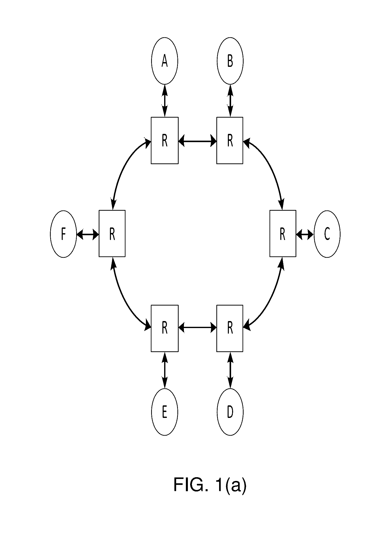
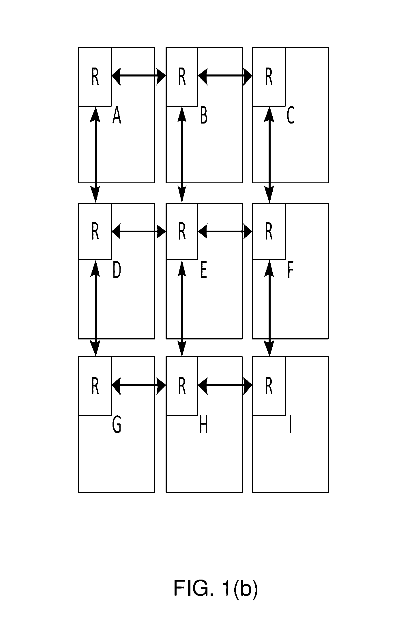
[0041]A distributed NoC interconnect connects various components of a system on chip (SoC) with each other using multiple routers and point to point links between the routers. Traffic profile of a SoC includes transactions between various components in the SoC and their properties (e.g., Quality of Service (QoS), priority, bandwidth and laten...


PUM


Abstract

The present disclosure relates system and method for automatic assignment of power domain and voltage domain to one or more SoC and/or NoC elements based on one or a combination of NoC and/or SoC specification/design, traffic specification, connectivity between SoC hosts that the NoC element in context is a part of, power specification (power domain and voltage domain of each host) of the hosts/SoC, and power profile(s) applicable for the NoC element in context. In another example implementation, power domain and voltage domain can be assigned to each SoC and/or NoC element based on pre-defined constraints and with an objective of reducing/minimizing static power consumption, reducing/minimizing hardware area, or identifying a tradeoff between the two parameters.

Description

BACKGROUND[0001]Technical Field[0002]Methods and example implementations described herein are directed to an interconnect architecture, and more specifically, to implementation of automatic power and voltage domain assignment to System on Chip (SoC) and / or Network on Chip (NoC) elements.[0003]Related Art[0004]The number of components on a chip is rapidly growing due to increasing levels of integration, system complexity and shrinking transistor geometry. Complex System-on-Chips (SoCs) may involve a variety of components e.g., processor cores, DSPs, hardware accelerators, memory and I / O, while Chip Multi-Processors (CMPs) may involve a large number of homogenous processor cores, memory and I / O subsystems. In both SoC and CMP systems, the on-chip interconnect plays a role in providing high-performance communication between the various components. Due to scalability limitations of traditional buses and crossbar based interconnects, Network-on-Chip (NoC) has emerged as a paradigm to int...

Claims


Application Information

Patent Timeline
Patent Type & Authority Patents(United States)
IPC IPC(8): G06F1/26G06F1/32
CPCG06F1/26G06F1/3253G06F1/3278G06F1/3287G06F1/3243G06F1/3296Y02D10/00
Inventor KUMAR, SAILESHNORIGE, ERICRAPONI, PIER GIORGIO
Owner INTEL CORP
Why Eureka
Try Eureka