Semiconductor device assessment apparatus

a technology of semiconductor devices and assessment apparatuses, which is applied in the direction of measurement devices, electronic circuit testing, instruments, etc., can solve the problems of further be difficult to observe an image, and difficult to confirm the position of the semiconductor substra

Active Publication Date: 2017-01-24
MITSUBISHI ELECTRIC CORP
View PDF15 Cites 0 Cited by
  • Summary
  • Abstract
  • Description
  • Claims
  • Application Information

AI Technical Summary

Benefits of technology

[0006]However, a semiconductor substrate may have a peripheral portion rounded as seen depthwise, inclined or the like, and it has thus been difficult to observe an image thereof to therefrom detect the semiconductor substrate's peripheral edge easily and precisely.
[0008]The present invention has been made to address the above issue. A main object of the present invention lies in providing a semiconductor device assessment apparatus that can detect the position of a semiconductor substrate on a holding unit with high precision.
[0010]The present invention thus contemplates a semiconductor device assessment apparatus that can detect the position of a semiconductor substrate on a holding unit with high precision.

Problems solved by technology

However, a semiconductor substrate may have a peripheral portion rounded as seen depthwise, inclined or the like, and it has thus been difficult to observe an image thereof to therefrom detect the semiconductor substrate's peripheral edge easily and precisely.
Furthermore, as the semiconductor substrate undergoes each step of a semiconductor device production method the semiconductor substrate has in-plane variation or the like in each step and thus no longer has a peripheral portion having uniform appearance or geometry, and it has thus further been difficult to observe an image thereof to therefrom detect the semiconductor substrate's peripheral edge easily and precisely.
It has thus been difficult to confirm the position of the semiconductor substrate on the stage via a semiconductor device assessment apparatus with high precision.

Method used


Image

  • Semiconductor device assessment apparatus
  • Semiconductor device assessment apparatus
  • Semiconductor device assessment apparatus

Examples


first embodiment

[0023

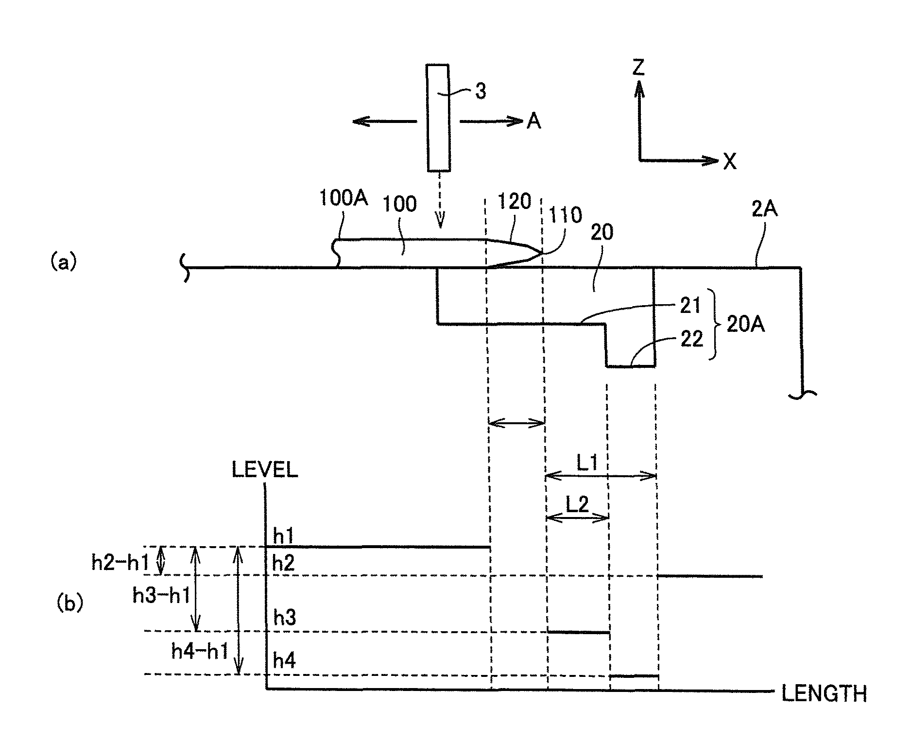
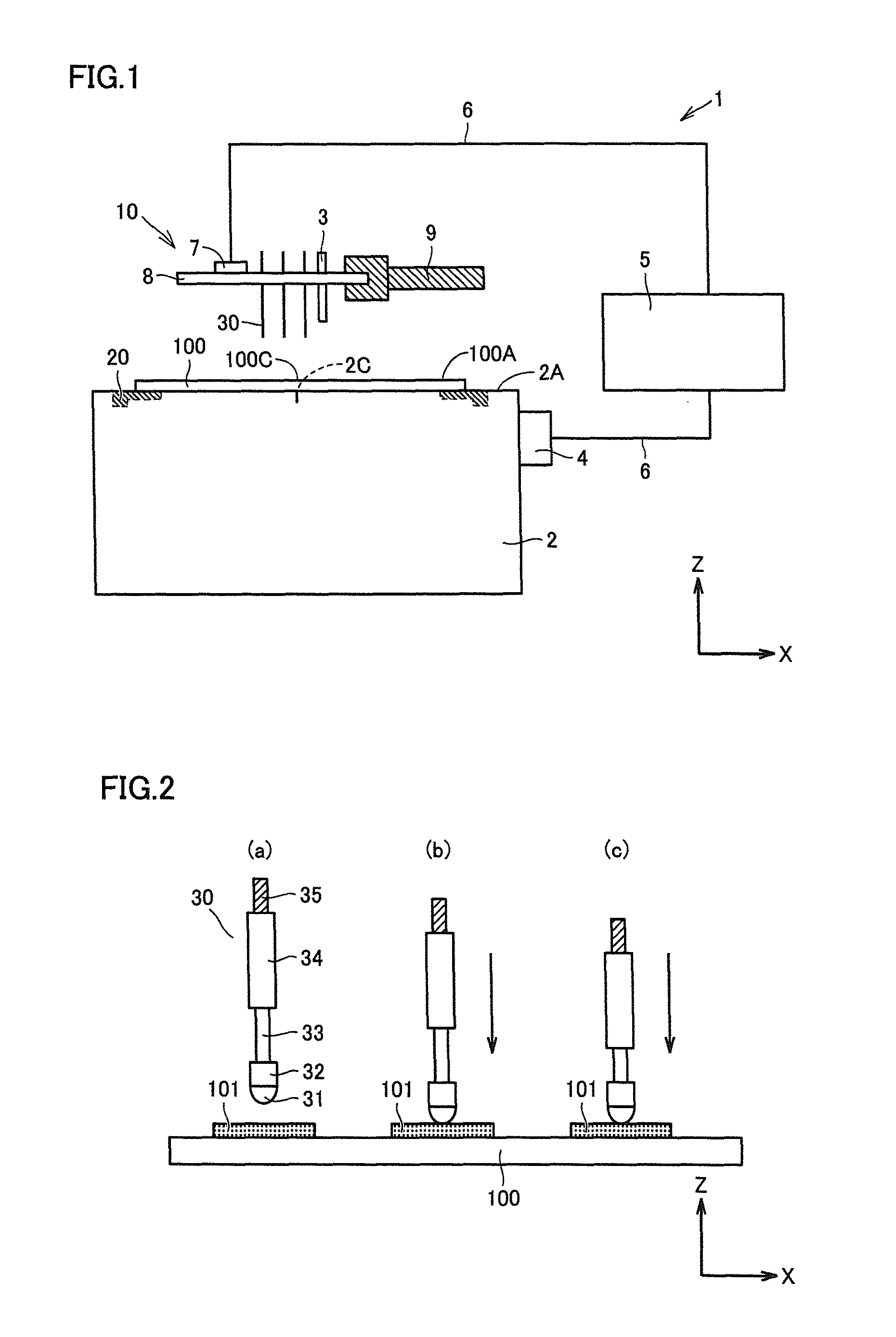
[0024]With reference to FIG. 1, a first embodiment provides a semiconductor device assessment apparatus 1 as will be described hereinafter. Semiconductor device assessment apparatus 1 is a semiconductor device assessment apparatus that electrically assesses a semiconductor device formed on a semiconductor substrate 100. In the present embodiment, semiconductor substrate 100 has a flat surface 100A with any semiconductor device formed thereon. This semiconductor device may for example be a vertical semiconductor device that passes a large current through semiconductor substrate 100 depthwise. Semiconductor device assessment apparatus 1 according to the present embodiment includes a holding unit 2 and a detection unit 3. Note that, in the present embodiment, a surface parallel to surface 2A of holding unit 2 is represented as an xy plane.

[0025]Holding unit 2 is configured to be capable of holding semiconductor substrate 100 on surface 2A. Holding unit 2 has surface 2A provided to...

second embodiment

[0045

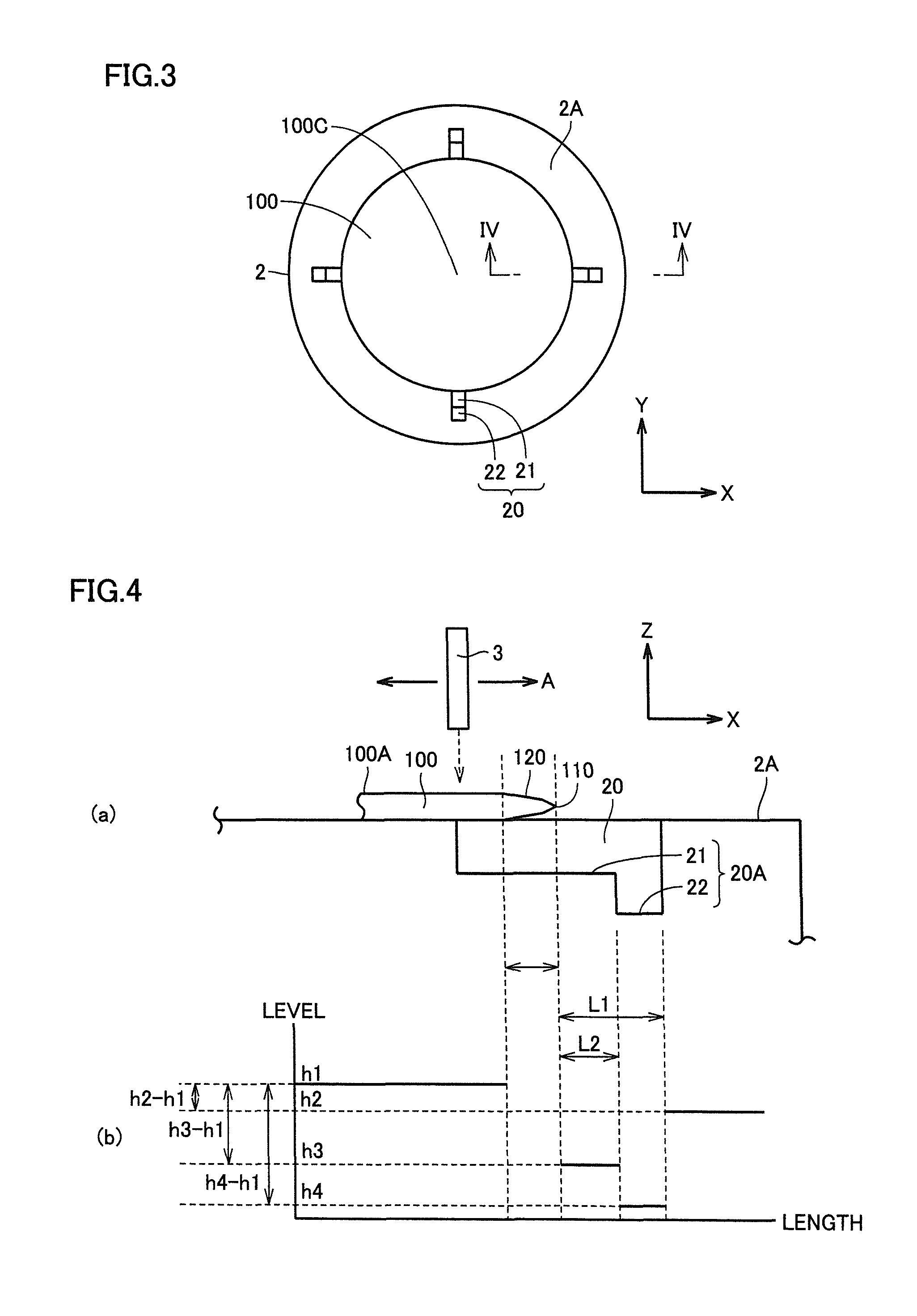
[0046]With reference to FIGS. 6-8, a second embodiment provides semiconductor device assessment apparatus 1, as will be described hereinafter. Semiconductor device assessment apparatus 1 according to the second embodiment is similar in configuration to that according to the first embodiment, except that the former has holding unit 2 having surface 2A with a receded portion thereon in a region adjacent to a periphery of semiconductor substrate 100 outwardly (or at a peripheral portion of surface 2A), with groove 20 formed in that receded portion.

[0047]The receded portion is provided at a position remote by a distance from reference position 2C of holding unit 2. More specifically, the receded portion is configured as follows: on surface 2A, an upper step 23 is provided in a circle with reference position 2C serving as a center thereof, and a lower step 24 is provided radially outer than upper step 23 to surround upper step 23 to serve as the receded portion.

[0048]Groove 20 overl...


PUM


Abstract

A semiconductor device assessment apparatus that electrically assesses a semiconductor device formed on a semiconductor substrate includes a holding unit having a surface to hold the semiconductor substrate thereon, and a detection unit to detect irregularity on the surface of the holding unit. The holding unit on the surface includes a plurality of grooves formed such that when the semiconductor substrate is held on the surface, the grooves overlap a periphery of the semiconductor substrate and also have a portion located outer than the periphery of the semiconductor substrate.

Description

BACKGROUND OF THE INVENTION[0001]Field of the Invention[0002]The present invention relates to a semiconductor device assessment apparatus, and more specifically to a semiconductor device assessment apparatus capable of positionally detecting a semiconductor device.[0003]Description of the Background Art[0004]In a semiconductor device production process, semiconductor devices formed on a semiconductor substrate may have their electrical characteristics assessed before the semiconductor substrate is diced into individual semiconductor devices. In this case, the semiconductor device is assessed via an assessment apparatus generally including a stage (or a holding unit) to hold the semiconductor substrate during an assessment and a probe electrically connected to a pad of the semiconductor device formed on the semiconductor substrate. In the assessment, the semiconductor substrate is previously disposed with its center positioned at a reference position on the stage. This allows a plura...

Claims


Application Information

Patent Timeline
Patent Type & Authority Patents(United States)
IPC IPC(8): G01R31/28H01L21/68G01B11/14G01B11/30
CPCG01R31/2891H01L21/681G01B11/14G01B11/30G01R31/2831
Inventor AKIYAMA, HAJIMEOKADA, AKIRAYAMASHITA, KINYA
Owner MITSUBISHI ELECTRIC CORP
Why Eureka
Try Eureka