Pixel circuit, driving method thereof and display device

a driving method and display device technology, applied in the field of display technology, can solve the problems of affecting the display effect of the whole image, difficult to achieve finer pixel resolution by compressing the pixel pitch, and more difficult to achieve fine pixel resolution. achieve the effect of reducing the number of data lines, improving the flexibility of touch, and reducing the cost of i

Active Publication Date: 2017-08-29
BOE TECH GRP CO LTD +1
View PDF11 Cites 5 Cited by
  • Summary
  • Abstract
  • Description
  • Claims
  • Application Information

AI Technical Summary

Benefits of technology

[0007]To overcome the shortcomings in the prior art, the technical problem to be solved by the present invention is to provide a pixel circuit, a driving method thereof, and a display device including the pixel circuit, which can reduce the number of transistors in a compensation circuit in the pixel circuit and the number of its required data lines in the prior art, thereby substantially compressing pixel pitches and reducing the cost of IC, and then enabling a current flowing through OLED in each pixel not to be affected by a threshold voltage Vth of a driving transistor thereof, and finally ensuring uniformity of image display.
[0009]the compensation unit is configured to adjust a drive voltage of a driving transistor in the drive unit, so as to eliminate the impact of a threshold voltage of the driving transistor on a current flowing through the light-emitting unit, and the data line is configured to provide a data signal to the driving transistor;
[0048]The beneficial effects of the present invention are as follow: the pixel circuit improves flexibility of the touch by integrating a capacitive touch function and a photosensitive touch function into a whole; the pixel circuit further combines the compensation units in the adjacent sub-pixel units into a whole, such that the adjacent sub-pixel units can share one data line (i.e., one data line controls the compensation units in the two sub-pixel units), thereby sharing the compensation unit to drive the two sub-pixel units. Hence, the number of the transistors in the compensation circuit and the number of the data lines may be reduced, the pixel pitch may be substantially compressed and the cost of IC is reduced, thereby obtaining higher image quality and higher PPI (Pixels Per Inch). Meanwhile, it solves the problem that inconsistent currents flowing through the OLED in the pixels caused by inconsistent threshold voltages (Vth) of the driving transistors in pixels due to manufacturing process and long time operation, thereby enabling the current flowing through the OLED in each pixel not to be affected by the threshold voltage Vth of the driving transistor, and finally ensuring uniformity of the image display. Moreover, the compensation unit ensures that there is no current flowing through the OLED in the reset phase and the drive phase of the pixel circuit, which indirectly prolongs the service life of the OLED.

Problems solved by technology

Moreover, due to the reasons of manufacturing process and aging of devices, the threshold voltages Vth of the driving TFTs in respective pixels may drift, i.e., the threshold voltages of the driving TFTs in respective pixels are inconsistent, easily resulting in different currents for the OLED flowing through the respective pixels due to the different threshold voltages of the driving TFTs thereof, so that a display brightness of a display screen is non-uniform, thereby affecting a display effect of the whole image.
In the case of meeting the driving requirements, considering many factors such as distribution space of the TFT, the Cs and the data line, the pixel circuit in the prior art makes it difficult to achieve a finer pixel resolution by compressing the pixel pitches.
However, the addition of the above two touch functions is bound to further increase the pixel pitch, which makes it more difficult to achieve a fine pixel resolution.

Method used


Image

  • Pixel circuit, driving method thereof and display device
  • Pixel circuit, driving method thereof and display device
  • Pixel circuit, driving method thereof and display device

Examples


first embodiment

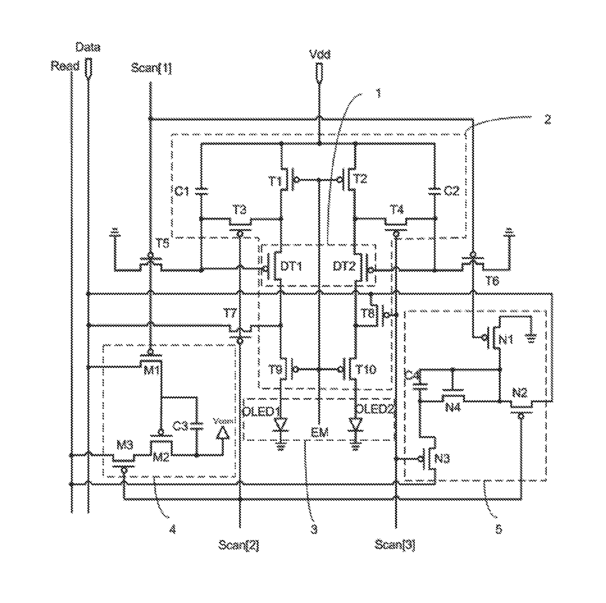
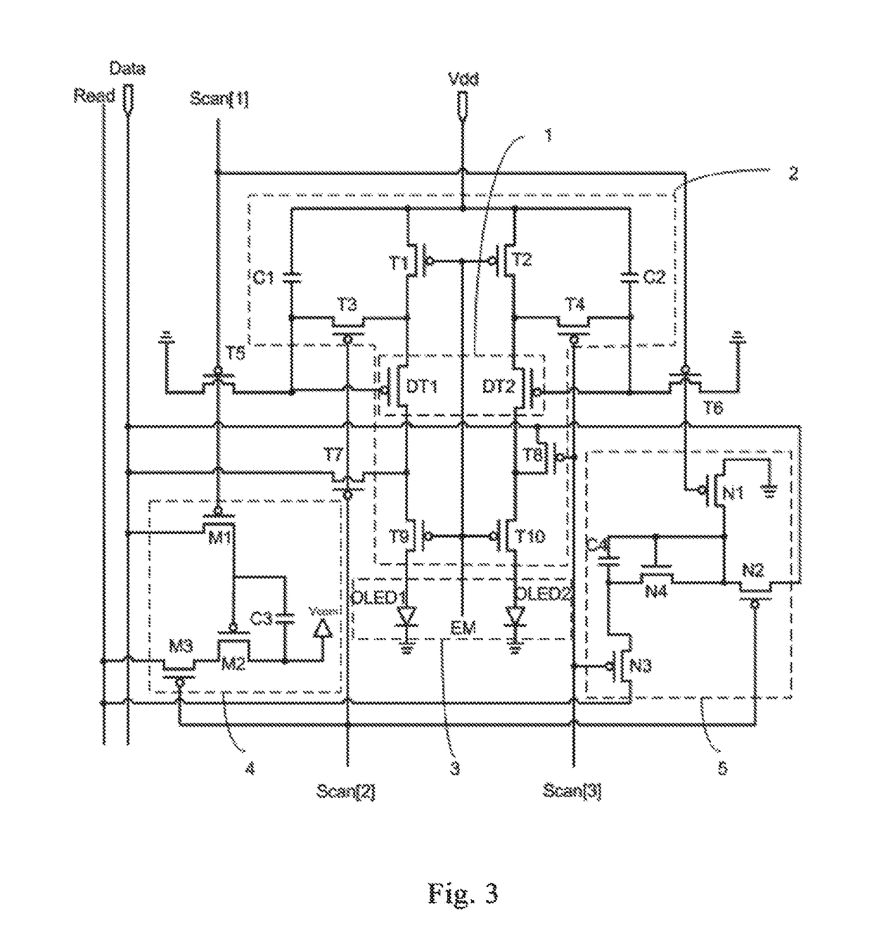
[0063]This embodiment provides a pixel circuit and a driving method corresponding to the pixel circuit.

[0064]As shown in FIG. 3, the pixel circuit includes a plurality of pixel structures, and each pixel structure is used for one sub-pixel unit. Specifically, the pixel circuit includes a drive unit 1, a compensation unit 2 and a light-emitting unit 3, wherein in the adjacent first pixel structure and second pixel structure, the drive unit 1 is composed of a drive unit in the first pixel structure and a drive unit in the second pixel structure, the compensation unit 2 is composed of a compensation unit in the first pixel structure and a compensation unit in the second pixel structure, and the light-emitting unit 3 is composed of a light-emitting unit in the first pixel structure and a light-emitting unit in the second pixel structure; the first pixel structure also includes a capacitive touch unit 4, and the second pixel structure also includes a photosensitive touch unit 5; and the ...

second embodiment

[0124]This embodiment provides a display device, including the pixel circuit in the first embodiment.

[0125]The display device includes a plurality of pixel structures arranged in a matrix form, the adjacent first pixel structure and second pixel structure may be adjacent sub-pixel units in the same pixel unit, or may be adjacent sub-pixel units in different adjacent pixel units. According to the design on the pixel unit in the display device, as shown in FIG. 6A, a pixel arrangement mode, in which the adjacent first pixel structure and second pixel structure are adjacent sub-pixel units in the same pixel unit, or as shown in FIG. 6B, a pixel arrangement mode, in which the adjacent first pixel structure and second pixel structure are adjacent sub-pixel units in different adjacent pixel units, may be designed according to actual needs.

[0126]In either of the above arrangement modes, the compensation unit in the first pixel structure, the compensation unit in the second pixel structure,...


PUM


Abstract

The present invention provides a pixel circuit comprising a plurality of pixel structures, each pixel structure comprising a drive unit, a compensation unit and a light-emitting unit, wherein in the adjacent first pixel structure and second pixel structure, the first pixel structure further comprises a capacitive touch unit, and the second pixel structure further comprises a photosensitive touch unit; the compensation unit in the first pixel structure, the compensation unit in the second pixel structure, the capacitive touch unit and the photosensitive touch unit share a data line, and the capacitive touch unit and the photosensitive touch unit share a read line.

Description

[0001]This is a National Phase Application filed under 35 U.S.C. 371 as a national stage of PCT / CN2014 / 086815, filed Sep. 18, 2014, an application claiming the benefit of Chinese Application No. 201410276701.8, filed Jun. 19, 2014, the content of each of which is hereby incorporated by reference in its entirety.FIELD OF THE INVENTION[0002]The present invention relates to the field of display technology, and particularly relates to a pixel circuit, a driving method thereof, and a display device including the pixel circuit.BACKGROUND OF THE INVENTION[0003]An organic light-emitting diode (OLED) display is one of the hot topics in the research field of flat-panel displays at present. Compared with a liquid crystal display (LCD), the OLED display has the advantages of low energy consumption, low production cost, self-luminescence, wide view angle, fast response and so on. At present, the OLED display has begun to gradually replace the traditional LCD in the display fields, such as mobile...

Claims


Application Information

Patent Timeline
Patent Type & Authority Patents(United States)
IPC IPC(8): G06F3/045G06F3/044G06F3/042G06F3/041G09G3/3233
CPCG06F3/044G06F3/042G06F3/0412G06F3/0416G09G3/3233G09G2310/0262G09G2360/14G06F2203/04105G09G2300/0804G06F3/04184H10K59/40G06F3/04166
Inventor YANG, SHENGJI
Owner BOE TECH GRP CO LTD
Why Eureka
Try Eureka