

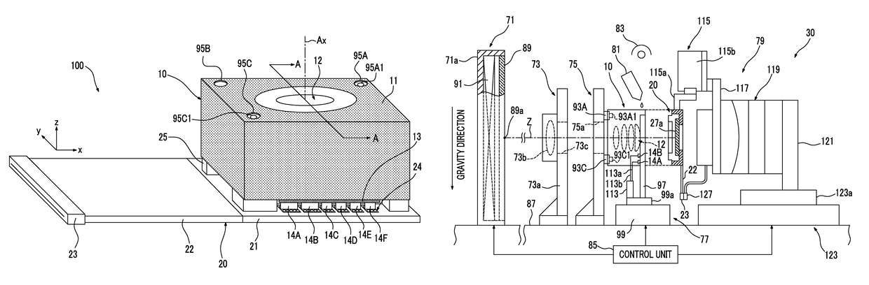
Imaging module and electronic device
a technology of imaging module and manufacturing method, which is applied in the direction of printers, instruments, cameras focusing arrangements, etc., can solve the problems of increasing the manufacturing cost of imaging modules and high cost of imaging modules, and achieve the effect of low cost and high accuracy
- Summary
- Abstract
- Description
- Claims
- Application Information
AI Technical Summary
Benefits of technology
Problems solved by technology
Method used
Image

Examples
first modification example
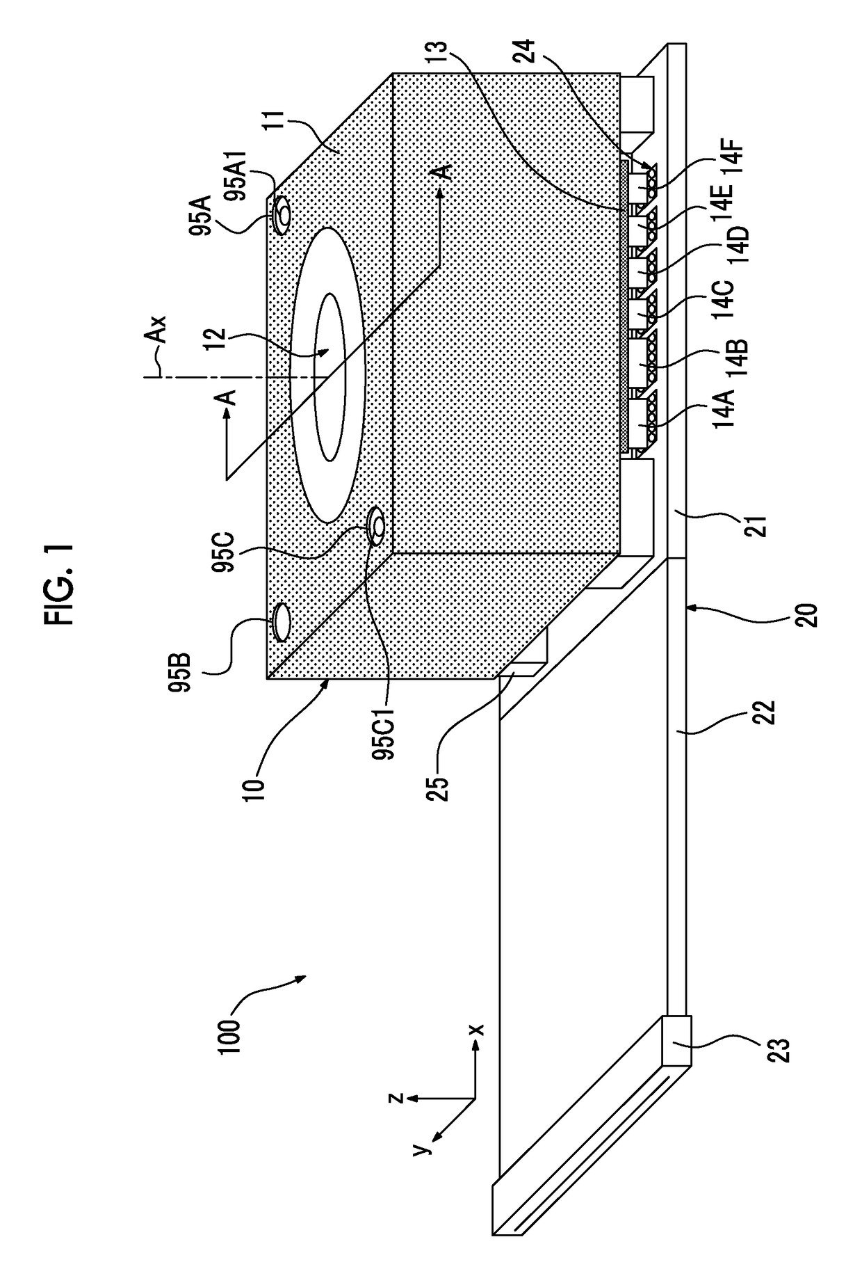
[0120]FIG. 7 is an external perspective view of an imaging module 200 which is a modification example of the imaging module 100.
[0121]The imaging module 200 has the same configuration as the imaging module 100 except that the positions of the terminals 14A and 14B included in the lens unit terminal portion of the lens unit 10 are changed.
[0122]In the imaging module 100, in the arrangement direction (x direction) of the terminals 14A to 14F included in the lens unit terminal portion, other terminals do not exist between the terminal 14A and the terminal 14B having a large exposed area. Meanwhile, in the imaging module 200, other terminals to which electricity does not flow during the adjustment process exist between the terminal 14A and the terminal 14B and are arranged therebetween.
[0123]According to this arrangement, it is possible to increase the distance between the terminals which come into contact with the probe pins during the adjustment process. Accordingly, an electrical con...
second modification example
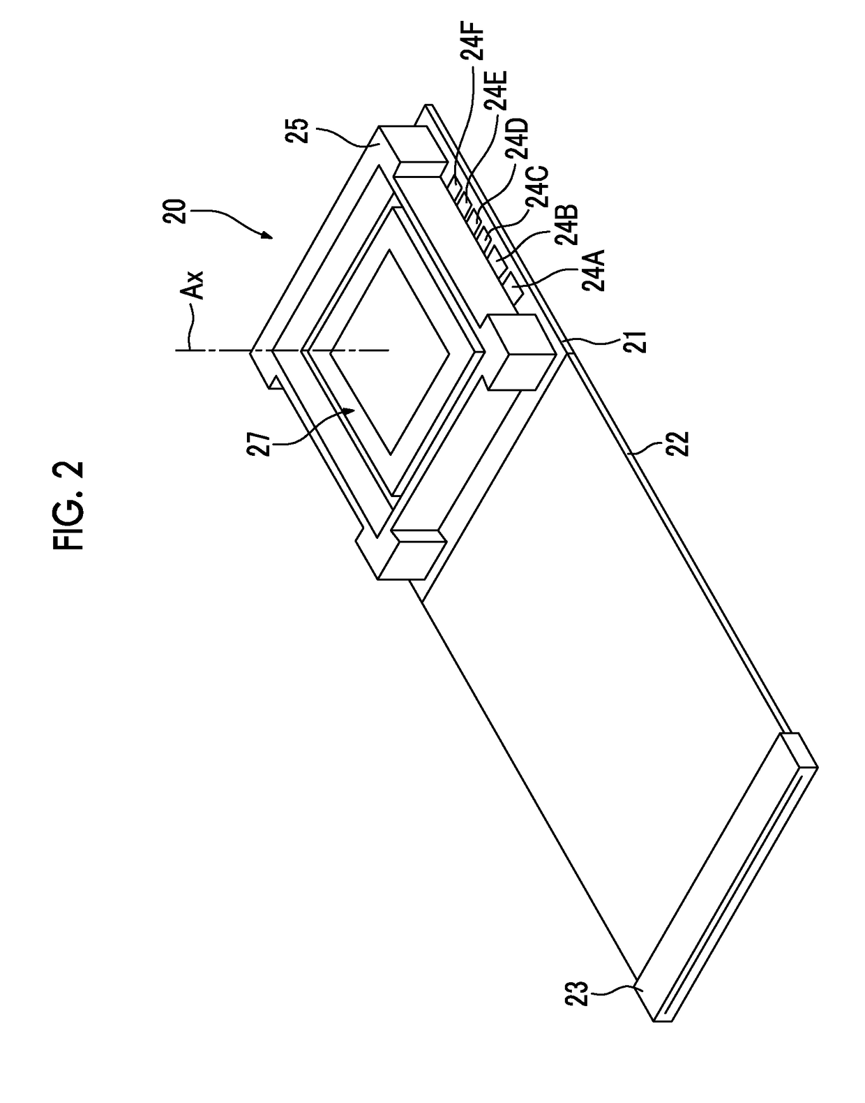
[0124]FIG. 8 is an external perspective view of an imaging module 300 which is a modification example of the imaging module 100.
[0125]In the imaging module 100, the terminal 14A to the terminal 14F included in the lens unit terminal portion are arranged in the direction along one side of outer edges of the imaging element 27 in a plan view. Meanwhile, the imaging module 300 is different from the imaging module 100 in that the terminal 14A to the terminal 14F are arranged in directions along two sides different from each other (in the example of FIG. 8, the side parallel to the x direction and the side parallel to the y direction in a plan view) of the outer edges of the imaging element 27 in a plan view.
[0126]Moreover, in the imaging module 300, the dispositions of the terminals 24A to 24F provided on the substrate 21 are changed according to the changes of the dispositions of the terminal 14A to the terminal 14F.
[0127]Among the terminals included in the lens unit terminal portion o...
third modification example
[0129]FIG. 9 is an external perspective view of an imaging module 400 which is a modification example of the imaging module 100.
[0130]The imaging module 400 has the same configuration as the imaging module 100 except that among the terminals included in the lens unit terminal portion of the lens unit 10, the exposed areas of the terminals 14A to 14D are larger than the exposed areas of the remaining terminals.
[0131]In a manufacturing apparatus for manufacturing the imaging module 400, in FIG. 5, the probe unit 113 is configured so as to include the probe pin for coming into contact with each of the terminals 14A to 14D.
[0132]Moreover, in this manufacturing apparatus, in a state where the second lens driving unit and the third lens driving unit are driven via the probe unit 113, and the position in the x direction and the position in the y direction of the lens group 12 are controlled so as to reach desired positions, the positioning of the lens unit 10 and the imaging element unit 2...
PUM
 Abstract
Description
Claims
Application Information