Image sensor device

a sensor device and image technology, applied in the field of integrated circuits, can solve the problems of affecting the performance of the camera, the amount of signal propagation delay,

Active Publication Date: 2018-02-20
INVENSAS LLC
View PDF13 Cites 48 Cited by
  • Summary
  • Abstract
  • Description
  • Claims
  • Application Information

AI Technical Summary

Problems solved by technology

Distance between an image sensor device and a separate chip coupled thereto, such as a controller or image sensor for example, of a camera causes an amount of signal propagation delay.
This delay can negatively impact performance of a camera.

Method used


Image

  • Image sensor device
  • Image sensor device
  • Image sensor device

Examples


Embodiment Construction

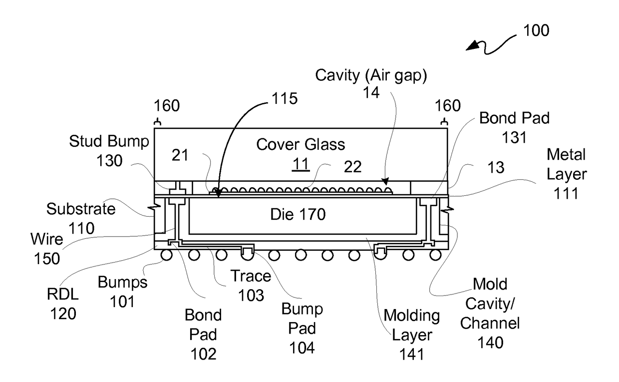
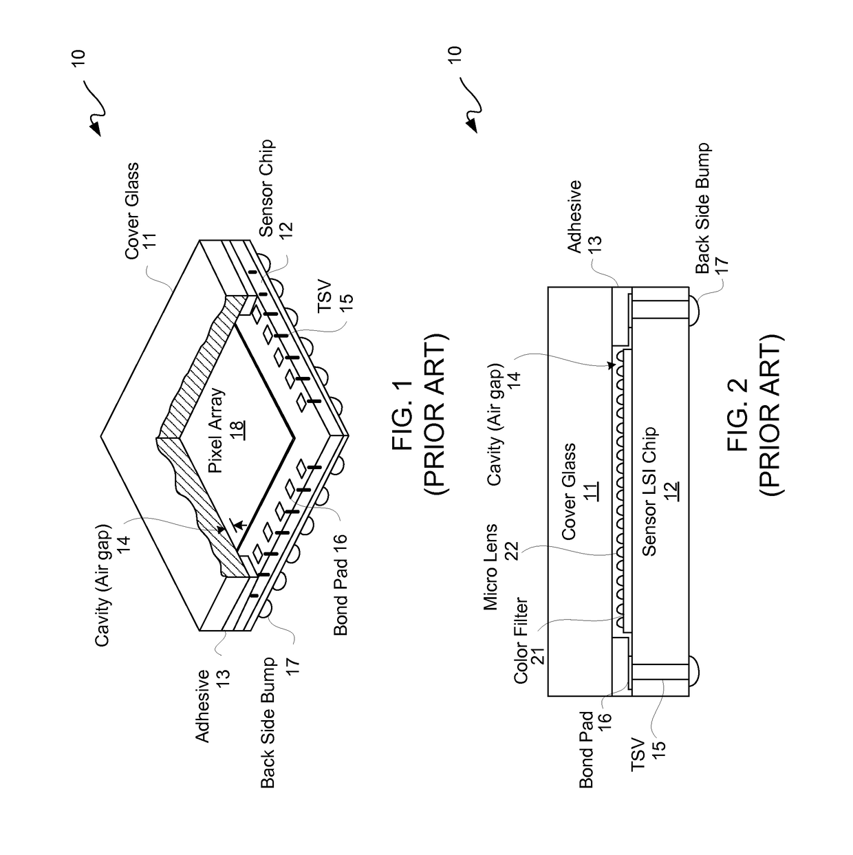
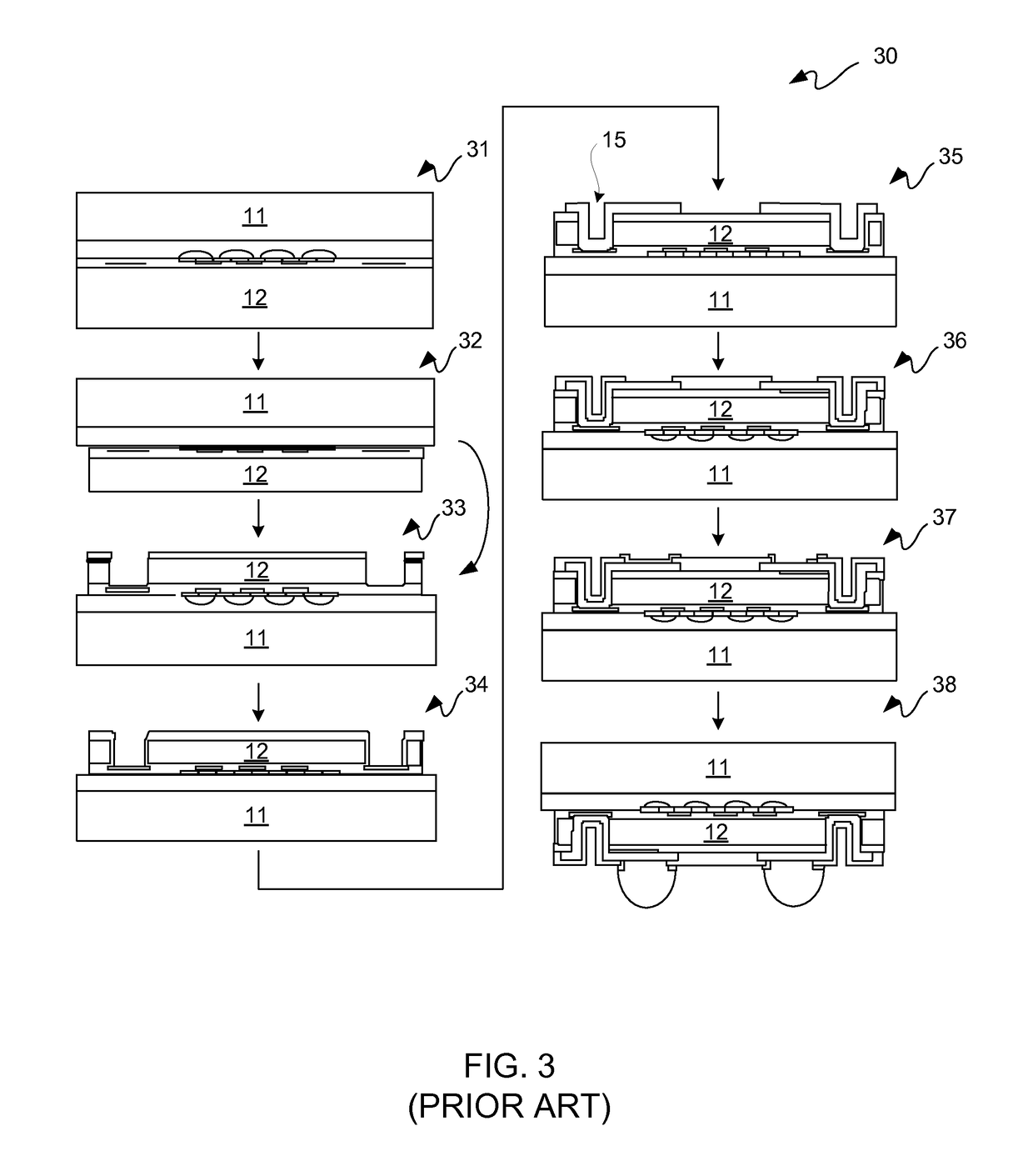
[0026]In the following description, numerous specific details are set forth to provide a more thorough description of the specific examples described herein. It should be apparent, however, to one skilled in the art, that one or more other examples or variations of these examples may be practiced without all the specific details given below. In other instances, well known features have not been described in detail so as not to obscure the description of the examples herein. For ease of illustration, the same number labels are used in different diagrams to refer to the same items; however, in alternative examples the items may be different.

[0027]Exemplary apparatus(es) and / or method(s) are described herein. It should be understood that the word “exemplary” is used herein to mean “serving as an example, instance, or illustration.” Any example or feature described herein as “exemplary” is not necessarily to be construed as preferred or advantageous over other examples or features.

[0028...


PUM


Abstract

An image sensor device, as well as methods therefor, is disclosed. This image sensor device includes a substrate having bond pads. The substrate has a through substrate channel defined therein extending between a front side surface and a back side surface thereof. The front side surface is associated with an optically-activatable surface. The bond pads are located at or proximal to the front side surface aligned for access via the through substrate channel. Wire bond wires are bonded to the bond pads at first ends thereof extending away from the bond pads with second ends of the wire bond wires located outside of an opening of the channel at the back side surface. A molding layer is disposed along the back side surface and in the through substrate channel. A redistribution layer is in contact with the molding layer and interconnected to the second ends of the wire bond wires.

Description

FIELD CROSS-REFERENCE TO RELATED APPLICATION(S)[0001]This application hereby claims priority to U.S. provisional patent application Ser. No. 62 / 090,788, filed on Dec. 11, 2014, the entirety of which is hereby incorporated by reference herein for all purposes.FIELD[0002]The following description relates to integrated circuits (“ICs”). More particularly, the following description relates to an image sensor device.BACKGROUND[0003]Microelectronic assemblies generally include one or more ICs, such as for example one or more packaged dies (“chips”) or one or more dies. One or more of such ICs may be mounted on a circuit platform, such as a wafer such as in wafer-level-packaging (“WLP”), printed board (“PB”), a printed wiring board (“PWB”), a printed circuit board (“PCB”), a printed wiring assembly (“PWA”), a printed circuit assembly (“PCA”), a package substrate, an interposer, or a chip carrier. Additionally, one IC may be mounted on another IC. An interposer may be an IC, and an interpos...

Claims


Application Information

Patent Timeline
Patent Type & Authority Patents(United States)
IPC IPC(8): H01L31/062H01L21/768H01L23/48H01L23/00H01L27/146
CPCH01L27/14634H01L21/76898H01L23/481H01L24/18H01L27/1469H01L27/14618H01L27/14636H01L27/14687H01L27/1464H01L2224/18H01L2224/19H01L2224/04105H01L2224/12105H01L2224/32145H01L2224/73267H01L2924/15153H01L2924/16235H01L2924/14H01L2924/19107H01L24/85H01L24/92H01L2224/92244H01L24/19H01L2924/00014H01L24/48H01L2224/05624H01L2224/45147H01L2224/45124H01L2224/45144H01L2224/45565H01L2224/45664H01L24/45H01L24/97H01L24/83H01L24/05H01L24/20H01L2224/32147H01L24/32H01L2924/00012H01L2224/29099
Inventor KATKAR, RAJESH
Owner INVENSAS LLC
Why Eureka
Try Eureka