
Semiconductor device having dummy active fin patterns

a technology of active fins and semiconductors, applied in the direction of instruments, cad circuit design, computer aided design, etc., can solve the problems of reducing yield and productivity

Active Publication Date: 2018-03-27
SAMSUNG ELECTRONICS CO LTD
View PDF39 Cites 5 Cited by
  • Summary
  • Abstract
  • Description
  • Claims
  • Application Information

AI Technical Summary

Benefits of technology

This approach enhances the semiconductor device manufacturing process by improving the margin for pattern formation in both circuit and dummy regions, reducing defects, and increasing productivity by ensuring appropriate density and spacing of patterns, thereby addressing the challenges of miniaturization and short channel effects.

Problems solved by technology

As miniaturized transistors having a FinFET structure are manufactured, unexpected defects may occur, thereby reducing yields and productivity.

Method used


Image

  • Semiconductor device having dummy active fin patterns
  • Semiconductor device having dummy active fin patterns
  • Semiconductor device having dummy active fin patterns

Examples


Embodiment Construction

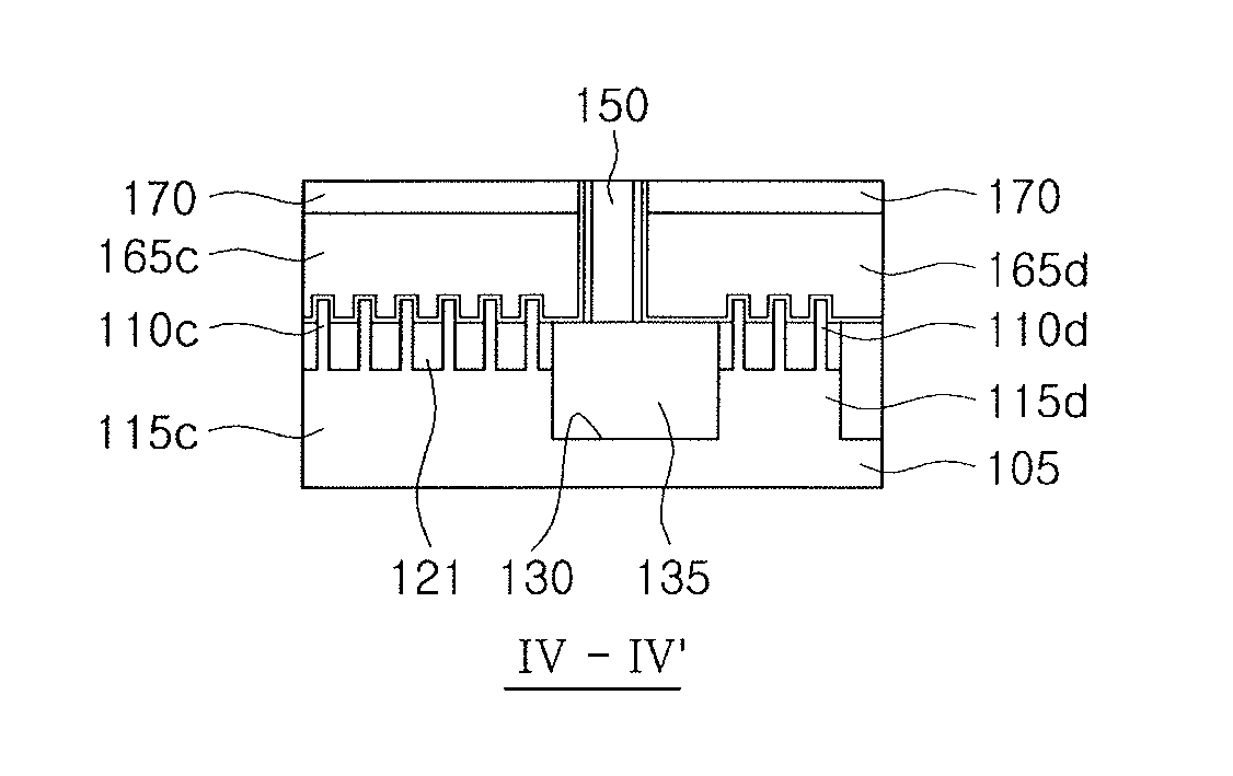
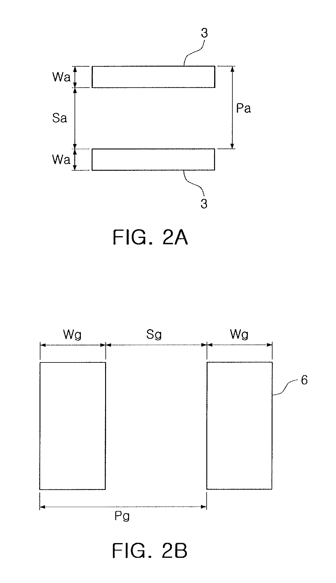
[0036]With reference to FIGS. 1 to 12, semiconductor device layout methods according to example embodiments, layouts formed using the layout methods, regions in which the layouts may be disposed, and target patterns for the formation of the layouts will be described below.

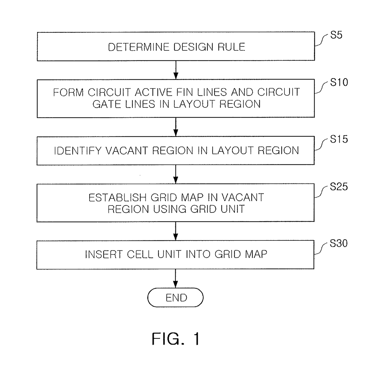
[0037]In FIGS. 1 to 12, FIGS. 1 to 9 are drawings illustrating semiconductor device layout methods according to example embodiments and layouts formed using the layout methods. FIGS. 10A to 10C are drawings illustrating regions in which layouts formed using semiconductor device layout methods according to example embodiments are disposed. FIGS. 11A to 12 are drawings illustrating an example of target patterns targeted at layouts in semiconductor device layout methods according to example embodiments.

[0038]First, a semiconductor device layout method according to an example embodiment will be described with reference to FIGS. 1 to 4B. In FIGS. 1 to 4B, FIG. 1 is a flowchart illustrating an example of a semiconductor ...


PUM


Abstract

A semiconductor device includes circuit active fin lines and circuit gate lines intersecting each other in a circuit active region, dummy active fin lines and dummy gate lines intersecting each other in a dummy active region, the active fin lines and the dummy active fin lines having same width and pitch, and the circuit gate lines and the dummy gate lines having same width and pitch, wherein at least some of the dummy active fin lines are aligned with and collinear with respective circuit active fin lines, and at least some of the dummy gate lines are aligned with and collinear with respective circuit gate lines.

Description

CROSS-REFERENCE TO RELATED APPLICATION[0001]Korean Patent Application No. 10-2016-0041563, filed on Apr. 5, 2016, in the Korean Intellectual Property Office, and entitled: “Layout Method and Semiconductor Device,” is incorporated by reference herein in its entirety.BACKGROUND1. Field[0002]Example embodiments relate to a layout method, a method of manufacturing a semiconductor device using the same, a semiconductor device thereof, and an electronic system selecting the same.2. Description of the Related Art[0003]As semiconductor devices tend to be highly integrated, transistors have gradually been miniaturized, and short channel effects of transistors are further increased. In order to suppress short channel effects, a fin field effect transistor (FinFET) structure has been proposed. As miniaturized transistors having a FinFET structure are manufactured, unexpected defects may occur, thereby reducing yields and productivity.SUMMARY[0004]In accordance with example embodiments, a layou...

Claims


Application Information

Patent Timeline
Patent Type & Authority Patents(United States)
IPC IPC(8): H01L27/08H01L23/52H01L27/02H01L29/66H01L23/528H01L27/088G06F17/50
CPCH01L27/0886H01L27/0207H01L23/528G06F17/5072G06F30/392G06F30/39H01L29/66795H01L29/0692H01L29/785H01L29/42372H01L29/42324
Inventor OH, IN WOOKYANG, JAE SEOKLEE, JONG HYUNLEE, HYUN JAEHWANG, SUNG WOOK
Owner SAMSUNG ELECTRONICS CO LTD
Learn More