Electronic circuit package

a technology of electronic circuits and components, applied in the direction of electrical apparatus, semiconductor devices, semiconductor/solid-state device details, etc., can solve the problems of difficult to solve malfunction, radio disturbance, malfunction and radio disturbance, etc., to prevent degradation of magnetic characteristics, easy and reliably connect metal films to power supply patterns, and high composite shielding

Active Publication Date: 2018-04-24
TDK CORPARATION
View PDF19 Cites 7 Cited by
  • Summary
  • Abstract
  • Description
  • Claims
  • Application Information

AI Technical Summary

Benefits of technology

[0006]The object of the present invention is therefore to provide an electronic circuit package having a composite shielding structure of both magnetic shielding function achieved by a magnetic film and electromagnetic shielding function by a metal film, capable of preventing degradation in magnetic characteristics of the magnetic film due to an eddy current.
[0008]According to the present invention, the resistance value at the interface between the magnetic film and the metal film is equal to or larger than 106Ω, so that an eddy current generated by electromagnetic wave noise entering the metal film hardly flows in the magnetic film. Therefore, it becomes possible to prevent degradation in magnetic characteristics of the magnetic film due to inflow of the eddy current.
[0009]In the present invention, the laminated structure preferably covers also a side surface of the molding resin. This can enhance composite shielding characteristics in the side surface direction.
[0011]In the present invention, the laminated structure is formed such that the magnetic film is positioned on the molding resin side. With this configuration, higher composite shielding characteristics can be obtained. However, the laminated structure may be formed such that the metal film is positioned on the molding resin side.
[0014]In the present invention, it is preferable that the power supply pattern is exposed to a side surface of the substrate and that the metal film contacts the exposed power supply pattern. With this configuration, it is possible to easily and reliably connect the metal film to the power supply pattern.
[0015]As described above, according to the present invention, it is possible to prevent degradation in magnetic characteristics of the magnetic film due to an eddy current while ensuring high composite shielding effect.

Problems solved by technology

However, this tendency poses a problem of malfunction and radio disturbance due to noise.
The problem of malfunction and radio disturbance is difficult to be solved by conventional noise countermeasure techniques.

Method used


Image

  • Electronic circuit package
  • Electronic circuit package
  • Electronic circuit package

Examples


first embodiment

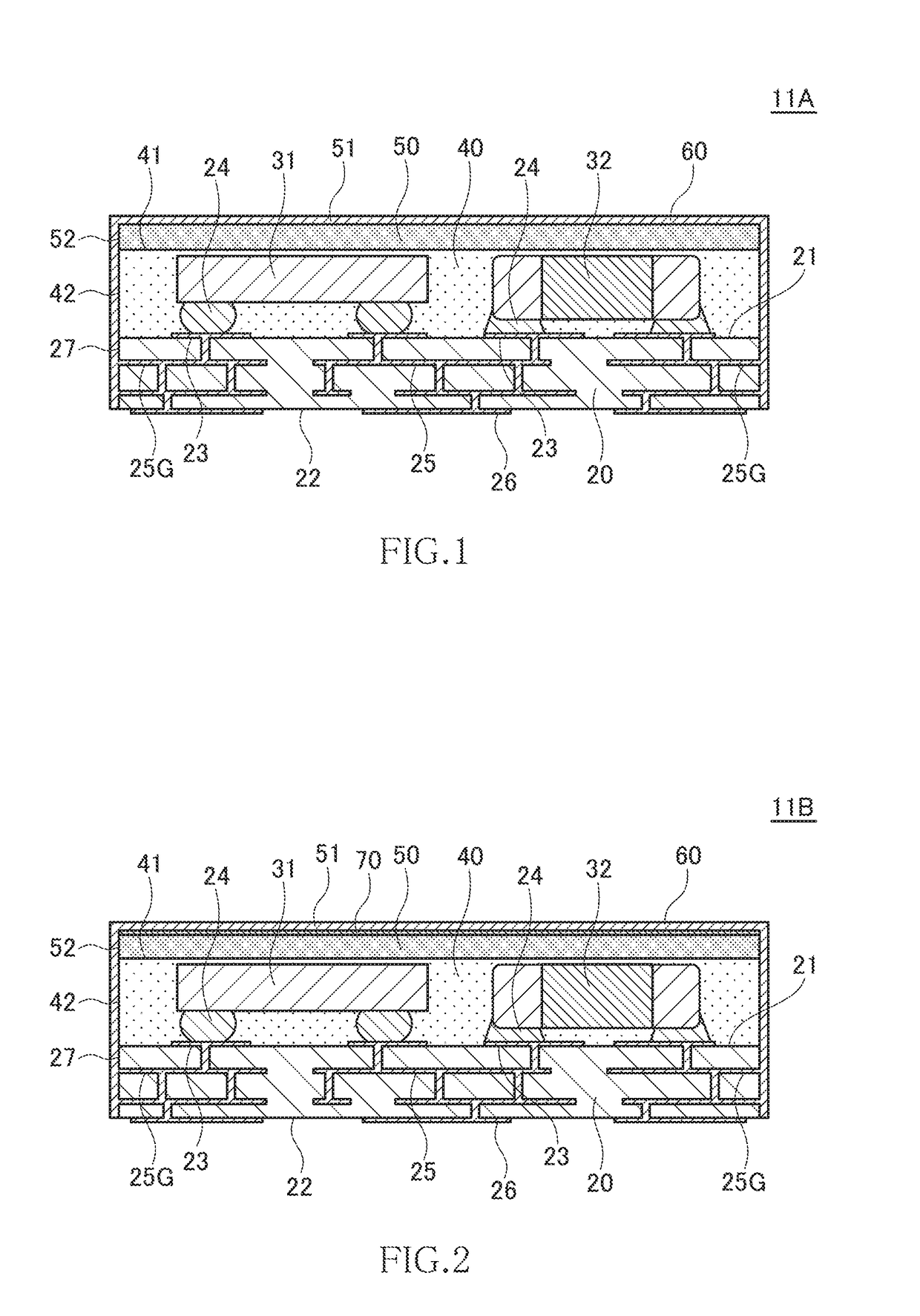
[0042]FIG. 1 is a cross-sectional view illustrating a configuration of an electronic circuit package 11A according to the first embodiment of the present invention.

[0043]As illustrated in FIG. 1, the electronic circuit package 11A according to the present embodiment includes a substrate 20, a plurality of electronic components 31 and 32 mounted on the substrate 20, a mold resin 40 covering a front surface 21 of the substrate 20 so as to embed the electronic components 31 and 32, a magnetic film 50 covering the mold resin 40, and a metal film 60 covering the mold resin 40 and the magnetic film.

[0044]Although the type of the electronic circuit package 11A according to the present embodiment is not especially limited, examples thereof include a high-frequency module handling a high-frequency signal, a power supply module performing power supply control, an SIP (System-In-Package) having a 2.5D structure or a 3D structure, and a semiconductor package for radio communication or digital c...

second embodiment

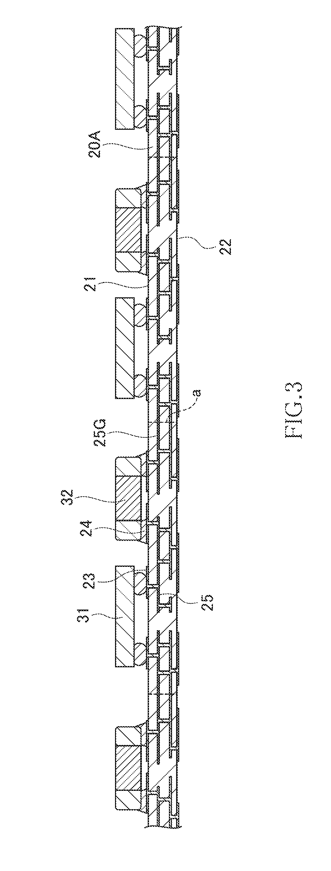
[0078]FIG. 11 is a cross-sectional view illustrating a configuration of an electronic circuit package 12A according to the second embodiment of the present invention.

[0079]As illustrated in FIG. 11, an electronic circuit package 12A according to the present embodiment is the same as the electronic circuit package 11A according to the first embodiment illustrated in FIG. 1 except for shapes of the substrate 20 and metal film 60. Thus, the same reference numerals are given to the same elements, and overlapping descriptions will be omitted.

[0080]In the present embodiment, the side surface 27 of the substrate 20 is formed stepwise. Specifically, a side surface lower portion 27b protrudes from a side surface upper portion 27a. The metal film 60 is not formed over the entire side surface of the substrate 20 but formed so as to cover the side surface upper portion 27a and a step portion 27c. The side surface lower portion 27b is not covered with the metal film 60. Also in the present embod...

third embodiment

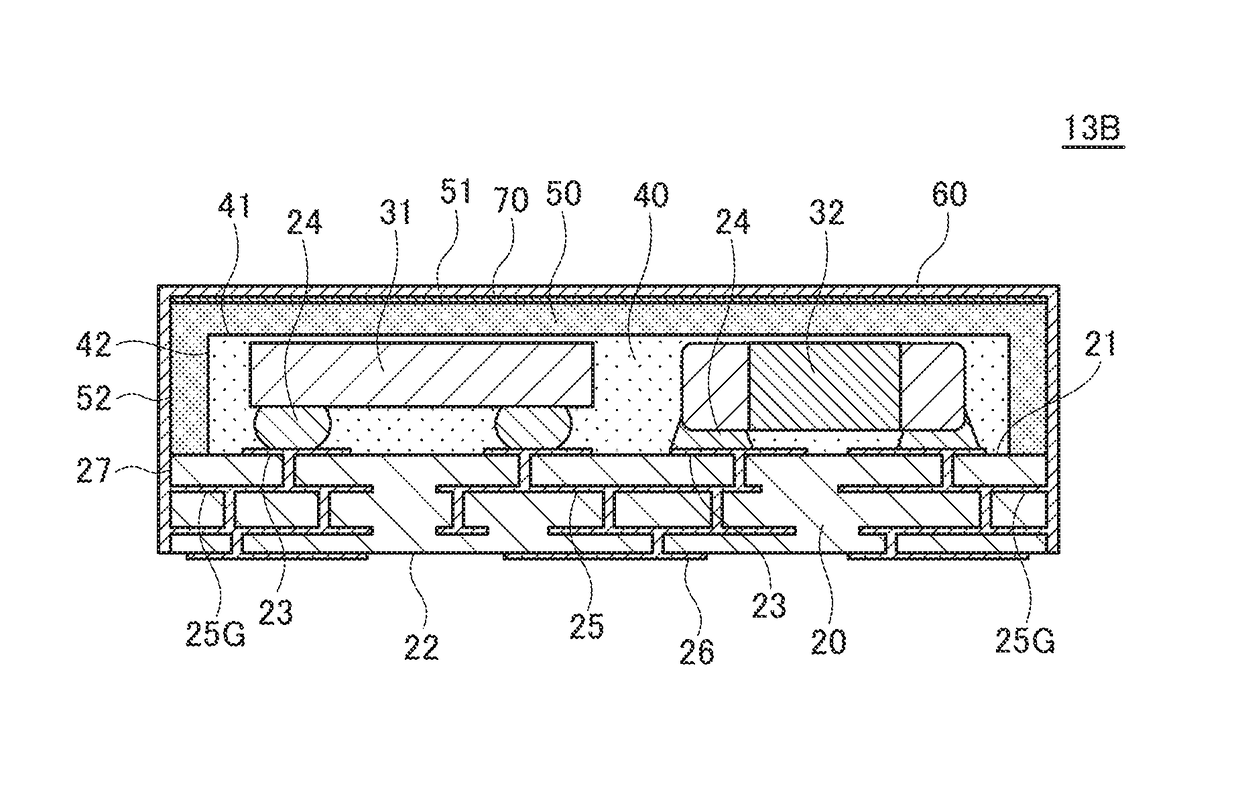
[0087]FIG. 17 is a cross-sectional view illustrating a configuration of an electronic circuit package 13A according to the third embodiment of the present invention.

[0088]As illustrated in FIG. 17, the electronic circuit package 13A according to the present embodiment differs from the electronic circuit package 11A according to the first embodiment illustrated in FIG. 1 in that the magnetic film 50 covers not only the top surface 41 of the mold resin 40, but also the side surface 42. Other configurations are the same as those of the electronic circuit package 11A according to the first embodiment. Thus, the same reference numerals are given to the same elements, and overlapping descriptions will be omitted.

[0089]In the present embodiment, the side surface 42 of the mold resin 40 is fully covered with the magnetic film 50, and thus, a part where the mold resin 40 and metal film 60 contact each other does not substantially exist. With this configuration, a composite-shield effect in t...


PUM


Abstract

Disclosed herein is an electronic circuit package includes: a substrate having a power supply pattern; an electronic component mounted on a surface of the substrate; a mold resin covering the surface of the substrate so as to embed therein the electronic component; a laminated structure of a magnetic film and a metal film, the laminated structure covering at least an upper surface of the molding resin. The metal film is connected to the power supply pattern, and a resistance value at an interface between the magnetic film and the metal film is equal to or larger than 106Ω.

Description

BACKGROUND OF THE INVENTIONField of the Invention[0001]The present invention relates to an electronic circuit package and, more particularly, to an electronic circuit package provided with a composite shielding function having both an electromagnetic shielding function and a magnetic shielding function.Description of Related Art[0002]In recent years, an electronic device such as a smartphone is equipped with a high-performance radio communication circuit and a high-performance digital chip, and an operating frequency of a semiconductor IC used therein tends to increase. Further, adoption of an SIP (System-In Package) having a 2.5D or 3D structure, in which a plurality of semiconductor ICs are connected by a shortest wiring, is accelerated, and modularization of a power supply system is expected to accelerate. Further, an electronic circuit module having a large number of modulated electronic components (collective term of components, such as passive components (an inductor, a capaci...

Claims


Application Information

Patent Timeline
Patent Type & Authority Patents(United States)
IPC IPC(8): H01L23/552H01L23/00H01L23/498H01L21/56H01L21/78H01L21/3205H01L23/31
CPCH01L23/552H01L21/565H01L21/78H01L23/3121H01L23/49838H01L24/16H01L24/97H01L21/32051H01L2924/3025H01L23/49822H01L23/49827H01L2224/16227H01L2924/0103H01L2924/01012H01L2924/01013H01L2924/01014H01L2924/01022H01L2924/01024H01L2924/01025H01L2924/01026H01L2924/01027H01L2924/01028H01L2924/01029H01L2924/0132H01L2924/0133H01L2924/01047H01L2924/01079H01L2924/05442H01L2924/19041H01L2924/19042H01L2924/19105H01L21/561H01L25/16H01L2224/16238H01L2224/81192H01L2224/97H01L2224/131H01L2924/15159H01L2924/15192H01L2924/15313H01L23/13H01L2224/81H01L2924/014
Inventor KAWABATA, KENICHIHAYAKAWA, TOSHIOOKUBO, TOSHIRO
Owner TDK CORPARATION
Why Eureka
Try Eureka