
Method for preparing Hf0.5Zr0.5O2 ferroelectric film by ALD for ferroelectric memory applications
A ferroelectric memory, ferroelectric thin film technology, applied in capacitors, electric solid devices, circuits, etc., can solve the problems of complex process, high preparation cost, large device size, etc., to simplify the preparation process and achieve uniform ferroelectricity of the thin film. , the effect of wide application prospects
Patent Information
- Authority / Receiving Office
- CN · China
- Patent Type
- Applications(China)
- Current Assignee / Owner
- Publication Date
- 2019-08-23
Smart Images
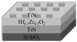
Figure 1 
Figure 2 
Figure 3
Abstract
Description
technical field
[0001] The invention belongs to the technical field of conductive materials, and in particular relates to an ALD preparation method for ferroelectric memory applications. 0.5 Zr 0.5 o 2 method for ferroelectric thin films. Background technique
[0002] Hafnium dioxide thin film is a high dielectric constant (High-K) material, which has the advantages of wide energy band gap and good compatibility with CMOS (Complementary Metal-Oxide-Semiconductor Transistor) process, and is widely used in micro Preparation of dielectric insulating materials in electronic devices. In recent years, studies have successively found that the dielectric material HfO 2 Doping with different elements will produce ferroelectricity, which can be used to prepare hafnium-based ferroelectric thin films. The traditional perovskite structure of Pb(Zr,Ti)O 3 (PZT), SrBi 2 Ta 2 o 9 (SBT) and other ferroelectric films, the development of ferroelectric memory is limited by factors such...
Examples
Embodiment 1
[0036] like Figure 7 Shown, the present invention prepares Si / SiO 2 The MIM structure capacitor method of / TiN / HZO / TiN is as follows:
[0037] 1. Processing substrate: select 15 mm 15mm with 100 nm SiO2 2The first-layer silicon wafer was used as the substrate, and was ultrasonically cleaned with acetone, isopropanol, and deionized water for 15 minutes in order to remove surface impurities, and finally dried with a nitrogen gun, and baked on a hot plate at 60 degrees for 5 minutes.
[0038] 2. Bottom electrode preparation: put the washed substrate into the magnetron sputtering chamber, Ti (99.995%) as the target material at 8*10 -4 The TiN thin film was grown under the vacuum of Pa, the substrate temperature was heated to 350 °C, and the sputtering current was 0.35 A. Sputter the Ti target in an argon atmosphere for 5 minutes to clean the target, then pass in nitrogen, Ar / N 2 The flow ratio is 15:1, sputter for 5 minutes, wait for the temperature to drop to room temperat...
Embodiment 2
[0057] 1. Processing substrate: select 15 mm 15 mm SiO-free 2 Layer P or N-type heavily doped silicon wafers as the substrate, ultrasonic cleaning with acetone, isopropanol, and deionized water for 15 minutes in sequence, cleaning impurities on the surface with a mixture of concentrated sulfuric acid and hydrogen peroxide, and removing silicon with HF acid. SiO formed on the sheet surface 2 , and finally blow dry with a nitrogen gun, put it on a hot plate and dry it at 60 degrees;
[0058] 2. Preparation of Hf 0.5 Zr 0.5 o 2 (HZO) Dielectric Thin Films: Fabrication of Hf Using Atomic Layer Deposition (ALD) 0.5 Zr 0.5 o 2 For the dielectric layer film, TDMAHf (tetradimethylammonium hafnium) and TDMAZr (tetradimethylammonium zirconium) are used as the reaction precursors respectively, ozone is used as the oxygen source, the chamber temperature is 280 °C, and the heating temperature of the source is 75 °C. Hafnium The Zr growth ratio is 1:1 (molar ratio), and the growth ...