
Low Temperature Sol-Gel Silicates As Dielectrics or Planarization Layers For Thin Film Transistors
Patent Information
- Authority / Receiving Office
- US · United States
- Current Assignee / Owner
- Publication Date
- 2008-01-17
- Estimated Expiration
- Not applicable · inactive patent
Smart Images
Figure 1 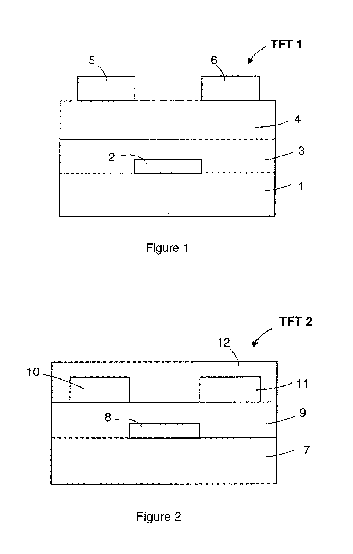
Figure 2 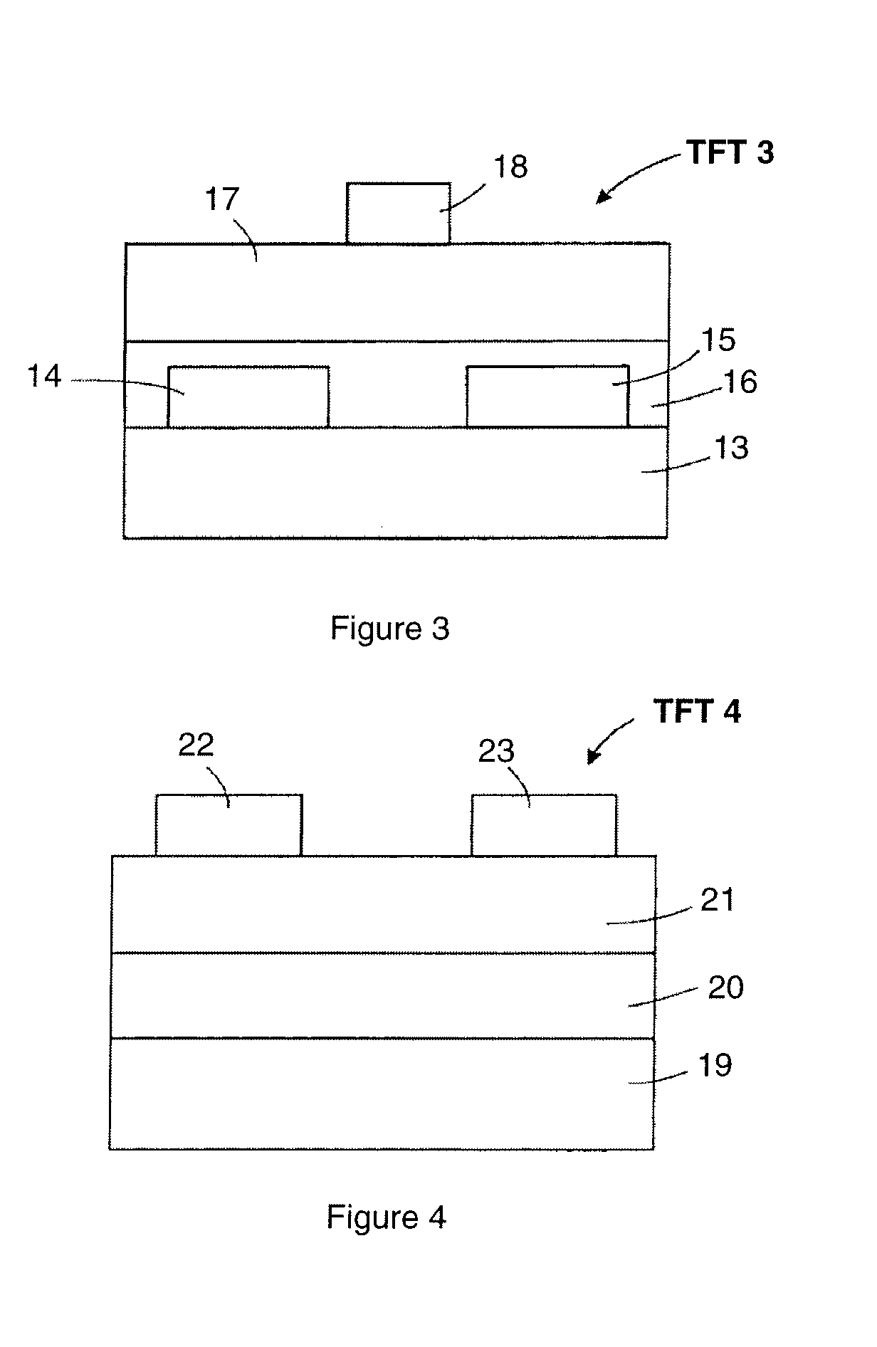
Figure 3
Abstract
Description
[0001] This Application claims the benefit of U.S. Provisional Application No. 60 / 831,161, filed on Jul. 14, 2006. The disclosure of this Provisional Application is hereby incorporated by reference. CROSS-REFERENCE TO RELATED APPLICATIONS
[0002] The subject matter of the instant invention is related to U.S. Patent Application Publication No. 2006 / 0097360A1, and U.S. patent application Ser. No. 11 / 752,722; both hereby incorporated by reference.BACKGROUND OF THE INVENTION
[0003] This invention relates to the use of low temperature processed sol-gel silica-containing formulations to provide silicate films at relatively low temperatures. In one aspect, films prepared from low temperature processing of these formulations can be used as gate dielectrics or interlayer dielectrics for thin film transistors (TFTs). In another aspect, higher temperature variants of these formulations may be used as planarization layers, for example, on stainless steel foils or substrates (e.g., TFTs on steel ...
Examples
example 1
Fabrication and Characterization of Gate Dielectric or Interlayer Dielectric for Thin Film Transistors
[0077] A dielectric film was prepared by combining 0.94 grams of methyltrimethoxysilane, 0.96 grams of triethoxysilane, and 0.13 grams of 3,3,3-trifluoropropyltrimethoxysilane and adding 2.50 grams of PGPE. This solution was shaken for three minutes. In a separate solution, 1.2 grams of 0.01M HNO3, and 0.02 g 0.1% by weight aqueous tetramethylammonium hydroxide solution were combined then added to the silane and solvent mixture. The solution was shaken for one minute and was homogeneous. The resulting solution was allowed to age for 6 days (ambient conditions) and 1 mL of it was filtered by through a 0.2μ filter before depositing it on a silicon wafer by spin coating at 500 rpm for 7 seconds then 1800 rpm for 40 seconds. The silicate-containing wafer was at 250° C. for 3 min. on a hot plate. The capacitance of the resulting 0.6μ layer was measured as 5 nF / cm2 via a mercury probe an...
example 2
Thin Film Transistor Fabrication
[0078] Thin film transistors are fabricated using silicate precursor solutions of Example 1 via spin-coating and printing techniques.
example 3
Planarization of Stainless Steel Foils
[0079] 1.61 g of methyltriethoxysilane, 1.61 g of tetraethoxysilane, 2.50 g of propylene glycol propyl ether, and 1.00 g of Triton X-114 were combined in a 30 g vial. To this mixture was added 1.71 g of 0.1M HNO3, followed by 0.07 g of 2.4 wt % TMAH, and the vial was shaken for 2 minutes. After aging the solution for 1 day, 2 mL of solution was applied via spin coating at a spin speed of 7 seconds at 500 rpm and 40 seconds at 1800 rpm onto a 6″ square stainless steel foil to give approximately a 1.4μ planarization film on the foil. The uncoated foil had an average rms roughness of 101 nm over a 25μ×25μ square area. The stainless steel foil containing the sol-gel silicate was then cured by heating the substrate to 90° C. for 90 seconds, to 180° C. for 90 seconds, and to 400° C. for 3 minutes on a hot plate. The now-planarized substrate rms roughness was an average of 13.25 nm rms roughness over a 25μ×25μ square area.