Device and methods for inspecting soldered connections

一种焊接点、地连接的技术,应用在测量装置、光学测试瑕疵/缺陷、仪器等方向,能够解决增加检查装置整体价格、透镜视野狭窄、棱镜易于损坏等问题

Inactive Publication Date: 2007-10-31
DELAWARE CAPITAL FORMATION INC
View PDF6 Cites 0 Cited by
  • Summary
  • Abstract
  • Description
  • Claims
  • Application Information

AI Technical Summary

Problems solved by technology

A drawback of this canon-style device is that the image reflected by the image transmission unit contains "interference", which will reduce the quality of the image
Another drawback of this Canon-type device is that the field of view of the lens is too narrow to visually inspect the upper and lower welds, and to be able to visually observe the upper and lower welds, the lens must be moved away from the weld The position of the point to provide a larger field of view, but this will reduce the clarity of the image
Another flaw of this Canon setup is that it uses a prism to reflect the image of the solder joint, we all know: prisms are easily damaged, so they need to be protected
Finally, these prisms are very expensive and thus will add to the overall price of the inspection unit and also require specially trained technicians to repair and / or maintain such prism components

Method used


Image

  • Device and methods for inspecting soldered connections
  • Device and methods for inspecting soldered connections
  • Device and methods for inspecting soldered connections

Examples


Embodiment Construction

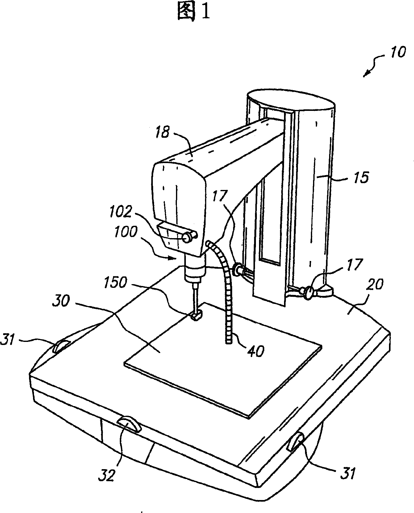
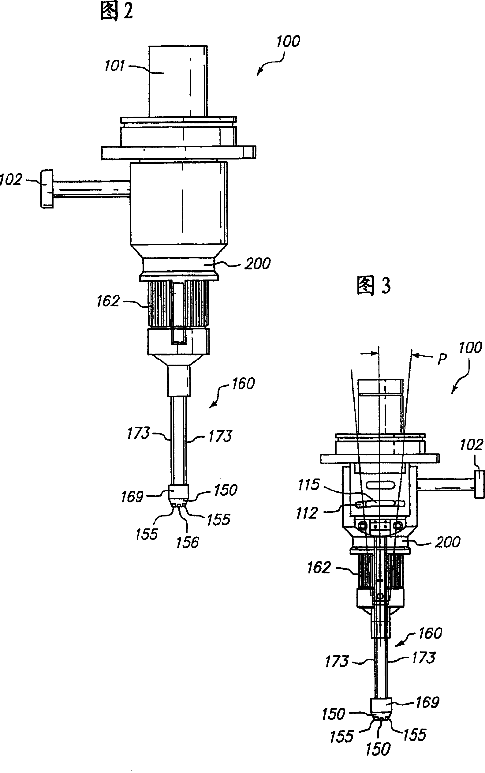
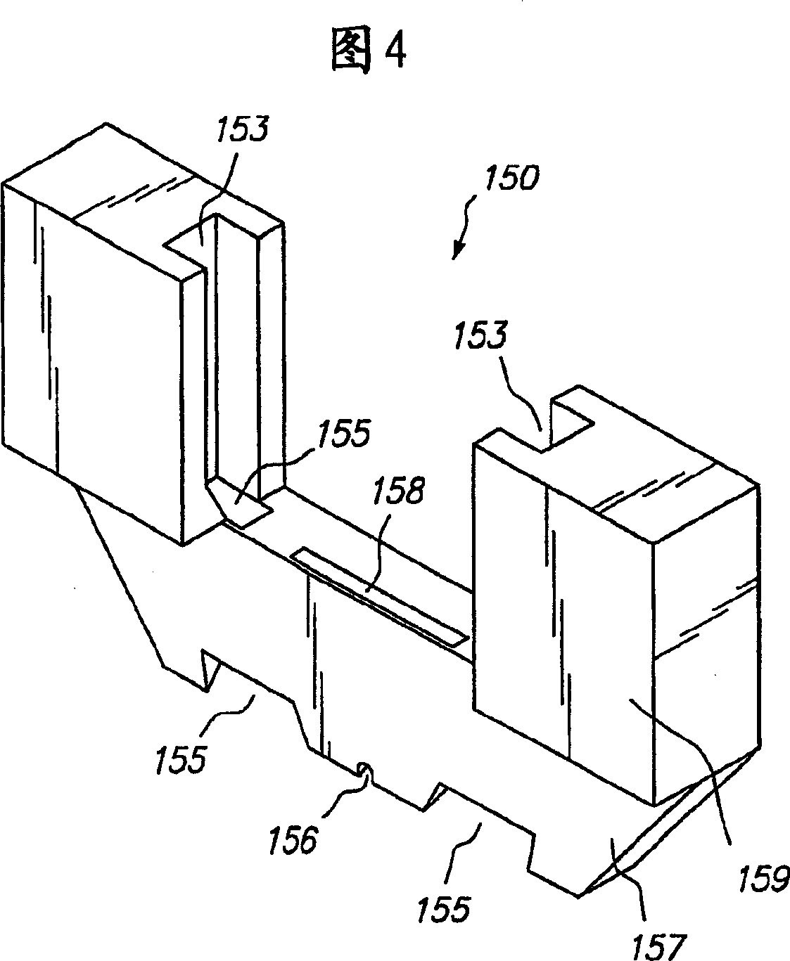
[0019] The invention includes an inspection device for inspecting the solder joints between a substrate and an integrated circuit. The detection device includes a base component and an optical inspection unit connected with the base. The base also includes a basically horizontal working area, in which a component to be checked is placed. The optical inspection unit can move in the vertical direction and can rotate relative to the working area.

[0020] Referring now to Figure 1, there is shown a detection device 10 according to the present invention. The inspection device 10 includes a base member 20 and an optical inspection unit 100. The base member 20 also includes a horizontal working surface 30, which can move relative to the optical inspection unit 100 along a vertical plane and a horizontal plane.

[0021] The working surface 30 can be moved by rotating the knobs 31 and 32, and the knobs 31 and 32 are operatively connected with the working surface 30 using well-known mechan...


PUM


Abstract

A device for inspecting solder connections between a component and a substrate or between two components or substrates, wherein the component is disposed upon the surface of the substrate, the device including an image receiving unit. An image transmitting device, the image transmitting device including a first end and a second end, the first end coupled to the image receiving unit. A tip assembly removably coupled to the second end of the image transmitting device, the tip assembly further including a mirror and an image receiving aperture, the tip assembly configured to transmit an image of the solder connections received by the mirror, through the image transmitting device, to the image receiving unit, and an illumination device, the illumination device including a light source, at least one light transmitting device, and at least one light emitting aperture disposed adjacent the image receiving aperture, the light emitting aperture directed towards the solder connections to be inspected.

Description

Technical field [0001] The present invention relates to a device and method for inspecting solder joints. Specifically, the device of the present invention can visually inspect hidden solder joints (for example, solder joints used to connect integrated circuits and printed circuit boards). checking. Background technique [0002] With the development of integrated circuit (ICs) technology, in addition to the ever-increasing density of integrated circuits used in electronic devices, surface-mounted integrated circuits, ball grid arrays (BGAs), chip-scale packages (CSPS) and flip-chips (FCs) The technology has also been greatly developed, so that it becomes more and more difficult to visually inspect the integrity of the solder joints between the chip leads and the solder joints on the printed circuit board. In addition, the number of solder joints on each chip is constantly increasing, while the size of the chip is constantly getting smaller. Although some surface-mounted integrate...

Claims


Application Information

Patent Timeline
Patent Type & Authority Patents(China)
IPC IPC(8): G01N21/956G01N21/88H05K13/08
CPCG01N21/8806
Inventor 格雷厄姆·罗斯
Owner DELAWARE CAPITAL FORMATION INC
Why Eureka
Try Eureka