PCB design method and system for automatically leading-in designing rules

A design method and rule-based technology, applied in the computer field, can solve the problems of reduced PCB design efficiency, difficulty in ensuring data accuracy, and inability to guarantee data, so as to reduce repetitive labor, ensure performance, and facilitate upgrade and maintenance.

Inactive Publication Date: 2008-01-09
HUAWEI TECH CO LTD
View PDF3 Cites 2 Cited by
  • Summary
  • Abstract
  • Description
  • Claims
  • Application Information

AI Technical Summary

Problems solved by technology

Therefore, the process of inputting design rules not only takes a lot of time, but also needs to comprehensively consider the enterprise specifications and the information conveyed by the production technologist, making it difficult to guarantee the accuracy of the data, and of course the data corresponding to the imported design rules cannot be guaranteed is the current optimal value
[0005] At the same time, for the PCB design rules input by CAD engineers, it takes a lot of time to check item by item when QA (Quality Assurance Engineer) checks the CAD engineer's design, which further reduces the efficiency of PCB design

Method used


Image

  • PCB design method and system for automatically leading-in designing rules
  • PCB design method and system for automatically leading-in designing rules

Examples


Embodiment Construction

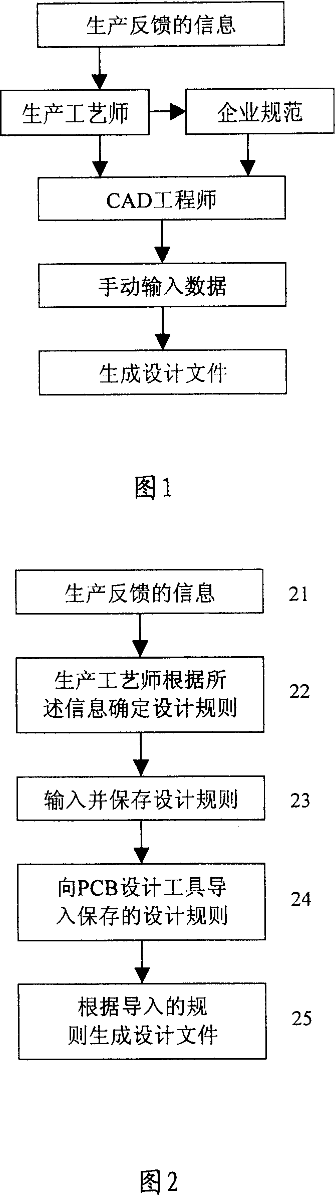
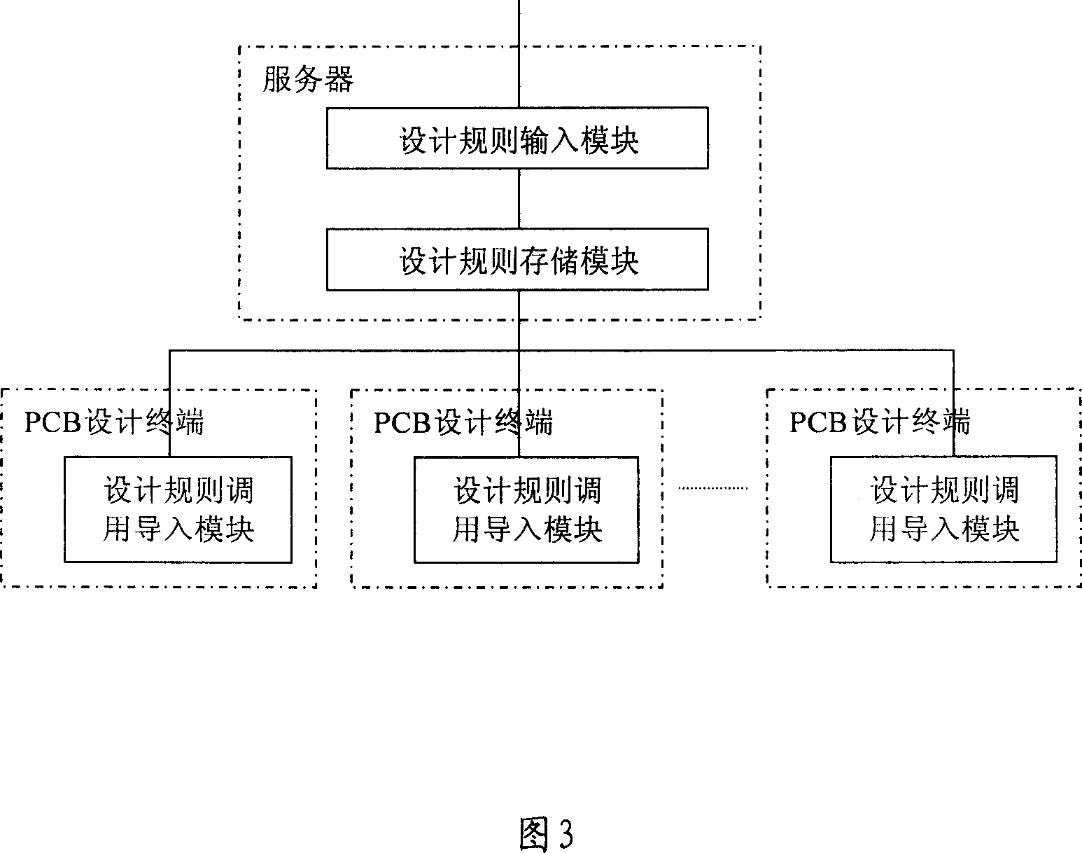
[0038] The core of the present invention is to save the design rules required by PCB design as a database file in a server that can be accessed by each PCB design terminal, such as the company's server. Save the design rules and import them into the corresponding PCB design files, so that the corresponding PCB design can be carried out based on the design rules. The design rules saved in the server are usually passed by the production technologist, CAD engineer expert, QA It is determined after analysis and evaluation by ICT engineers and others. Therefore, the accuracy of the design rules can be well guaranteed, and at the same time, the determined design rules can be guaranteed to be optimal. In the present invention, after the design rule is determined, it only needs to be input once and saved in the server, and then it can be updated in real time or periodically. , no need to manually enter the corresponding data.

[0039] Referring to Fig. 2, the PCB design method of the...


PUM


Abstract

The invention relates to method and system for design of a PCB (printed circuit board) that can lead in design rule automatically. In this invention, design rules, which are required by PCB design, as data base files are stored in server that is available for any PCB design terminal. When a CAD engineer proceeds with PCB design via PCB design terminal, said design rules are led in PCB design file and then the PCB design commences.

Description

technical field [0001] The invention relates to the technical field of computers, in particular to a PCB (printed circuit board) design method and system for automatically importing design rules. Background technique [0002] During the PCB design process, it is usually necessary to follow the corresponding design rules, such as the allowable spacing between device connections, the allowable width of the connection lines, etc. The design rules are usually recorded in the enterprise specifications, and the PCB design process is based on Enterprise norms are carried out. At present, the process of introducing the design rules adopted is shown in Figure 1, including: the production technologist formulates the enterprise specification for PCB design according to the feedback information in the PCB production process, and the PCB designer, namely CAD (Computer Aided Design) ) Engineers introduce design rules according to enterprise specifications, and carry out PCB design based ...

Claims


Application Information

Patent Timeline
Patent Type & Authority Patents(China)
IPC IPC(8): G06F17/50
Inventor 李广生梁伟宁
Owner HUAWEI TECH CO LTD
Why Eureka
Try Eureka