

Electronic device for the embedded semiconductor encapsulation part
A technology for electronic devices and packages, applied in semiconductor devices, semiconductor/solid-state device parts, electric solid-state devices, etc., can solve problems such as inconvenience, high defect rate, and general products without structure.
- Summary
- Abstract
- Description
- Claims
- Application Information
AI Technical Summary
Problems solved by technology
Method used
Image

Examples
Embodiment Construction
[0055] In order to further explain the technical means and effects that the present invention takes to achieve the intended purpose of the invention, the specific implementation, structure, Features and their functions are described in detail below.
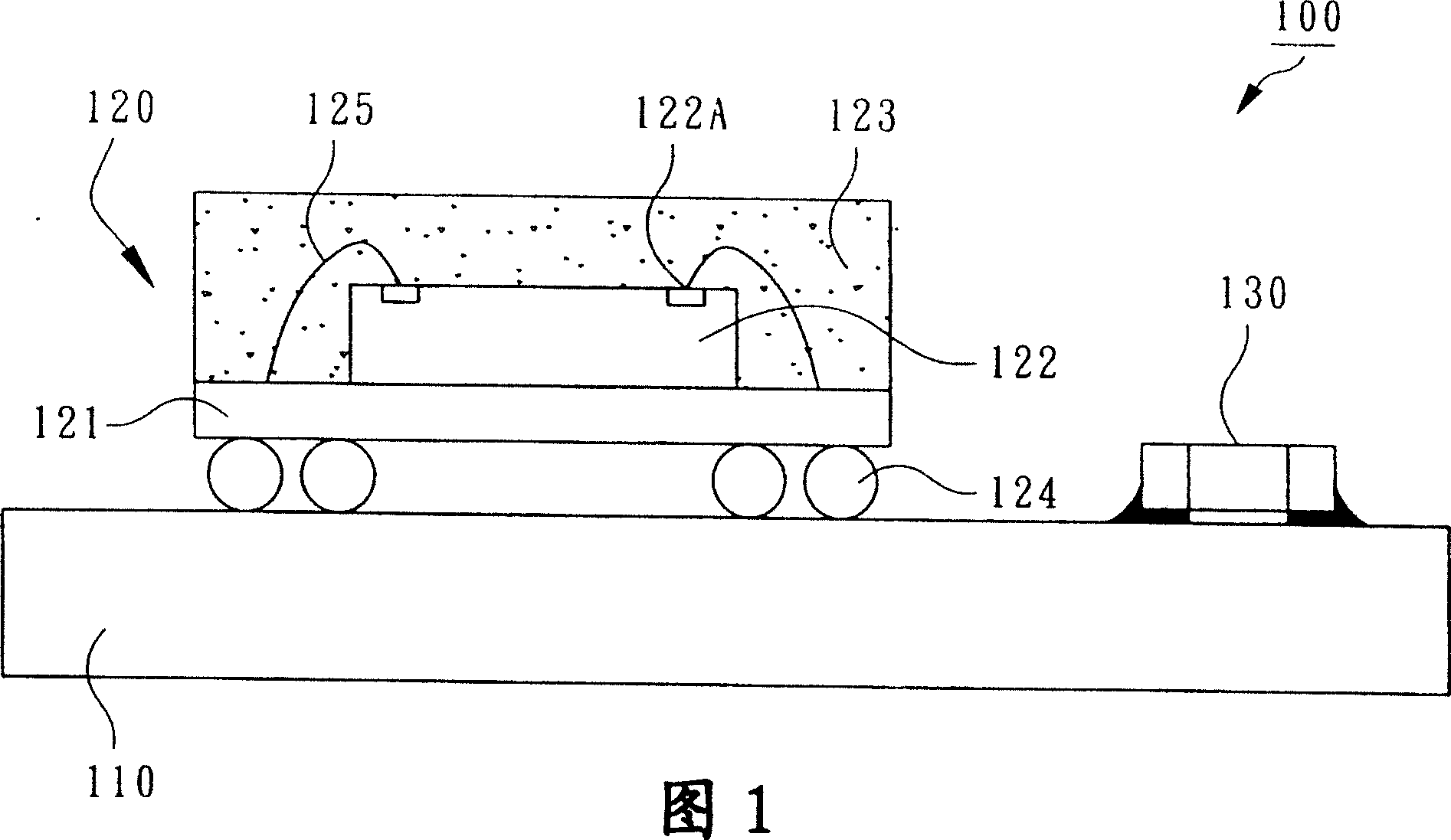
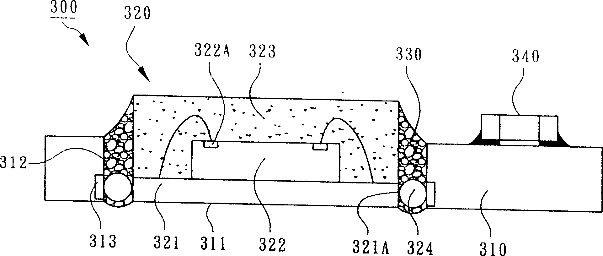
[0056] In the first specific embodiment of the present invention, such as image 3 and Figure 4 , discloses an electronic device 300 embedded with a semiconductor package.
[0057] see image 3 and Figure 4 as shown, image 3 is a schematic cross-sectional view of a first embodiment of an electronic device embedded with a semiconductor package according to the present invention, Figure 4 is a top view diagram. The electronic device 300 mainly includes a printed circuit board 310 and at least one semiconductor package 320, wherein:
[0058] The printed circuit board 310 has at least one cavity 311 , and at least one side wall 312 of the cavity 311 is formed with a plurality of internal terminals 313 , such as side metal pad...
PUM
 Abstract
Description
Claims
Application Information