Programmable non-volatile semiconductor memory device
A storage device and semiconductor technology, applied in static memory, read-only memory, information storage, etc., can solve the problem of large storage area of storage devices
- Summary
- Abstract
- Description
- Claims
- Application Information
AI Technical Summary
Problems solved by technology
Method used
Image

Examples
Embodiment Construction
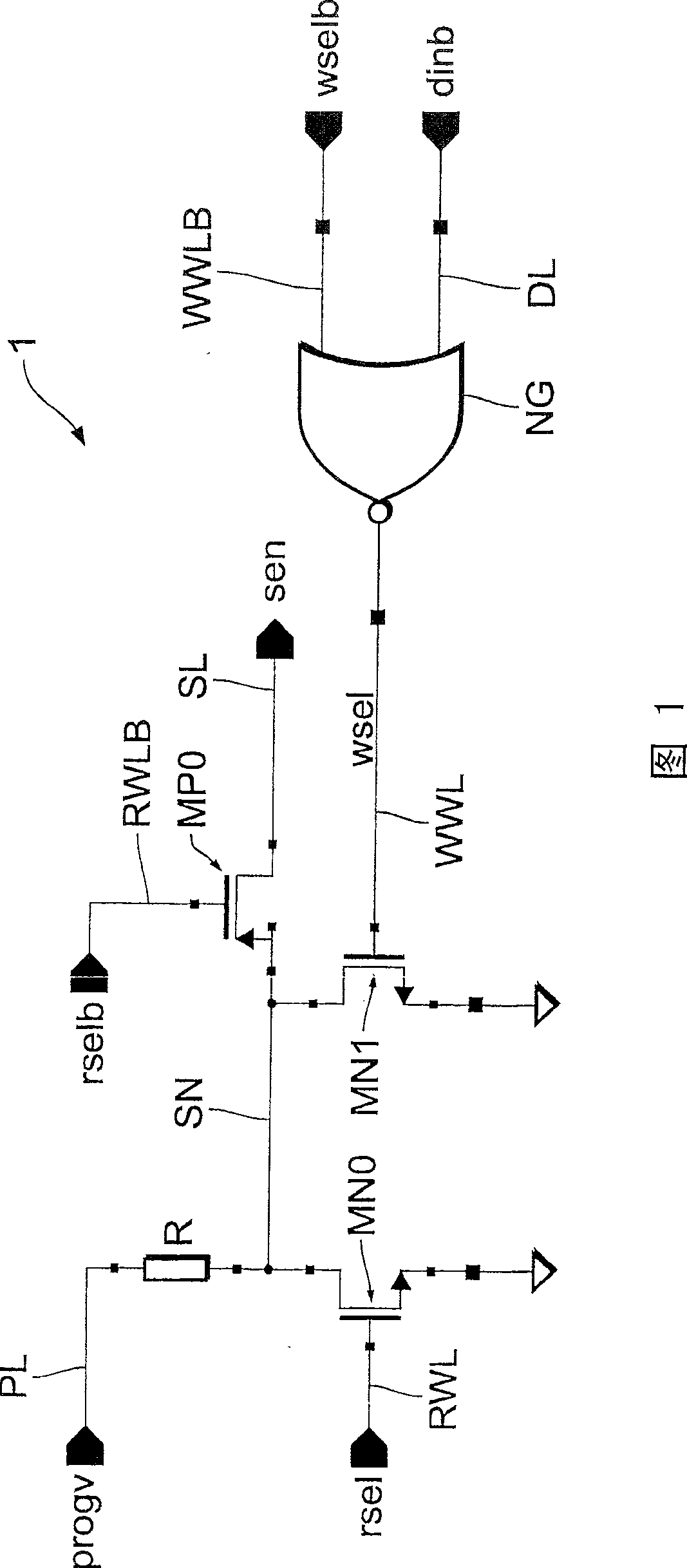
[0026] Fig. 1 shows a preferred embodiment of a circuit diagram of a memory cell 1 according to the invention. It comprises two bridge transistors MN0, MN1 with their drains connected together and their sources both connected to ground voltage level. The first bridge transistor MN0 may be controlled by a first selection signal, in particular, a read selection signal rsel provided on the read word line RWL. The second bridge transistor MN1 can be controlled by a second selection signal, in particular, a write selection signal wsel provided on the write word line WWL. The common drain connection of said transistors MN0, MN1 is hereinafter referred to as a sense node SN, which is connected to a first end of a silicided polysilicon fuse resistor R, which fuse resistor R The other end of is connected to the program line PL, and the program line PL is used to provide a programming signal progv for programming the memory cell 1 .
[0027] The memory cell 1 also includes a read tran...
PUM
 Abstract
Description
Claims
Application Information
 - R&D
- Intellectual Property
- Life Sciences
- Materials
- Tech Scout
- Unparalleled Data Quality
- Higher Quality Content
- 60% Fewer Hallucinations
Browse by: Latest US Patents, China's latest patents, Technical Efficacy Thesaurus, Application Domain, Technology Topic, Popular Technical Reports.
© 2025 PatSnap. All rights reserved.Legal|Privacy policy|Modern Slavery Act Transparency Statement|Sitemap|About US| Contact US: help@patsnap.com