Reference sense amplifier for non-volatile memory

a reference sense amplifier and non-volatile memory technology, applied in static storage, digital storage, instruments, etc., to achieve the effects of high capacity, high density chip integration, and high performance non-volatile memory devices

Inactive Publication Date: 2006-07-20
SANDISK TECH LLC
View PDF78 Cites 375 Cited by
  • Summary
  • Abstract
  • Description
  • Claims
  • Application Information

AI Technical Summary

Benefits of technology

[0041] These needs for a high capacity and high performance non-volatile memory device are met by having a large page of read/write circuits to read and write a corresponding page of memo...

Problems solved by technology

Source line bias is an error introduced by a non-zero resistance in the ground loop of the r...

Method used


Image

  • Reference sense amplifier for non-volatile memory
  • Reference sense amplifier for non-volatile memory
  • Reference sense amplifier for non-volatile memory

Examples


Embodiment Construction

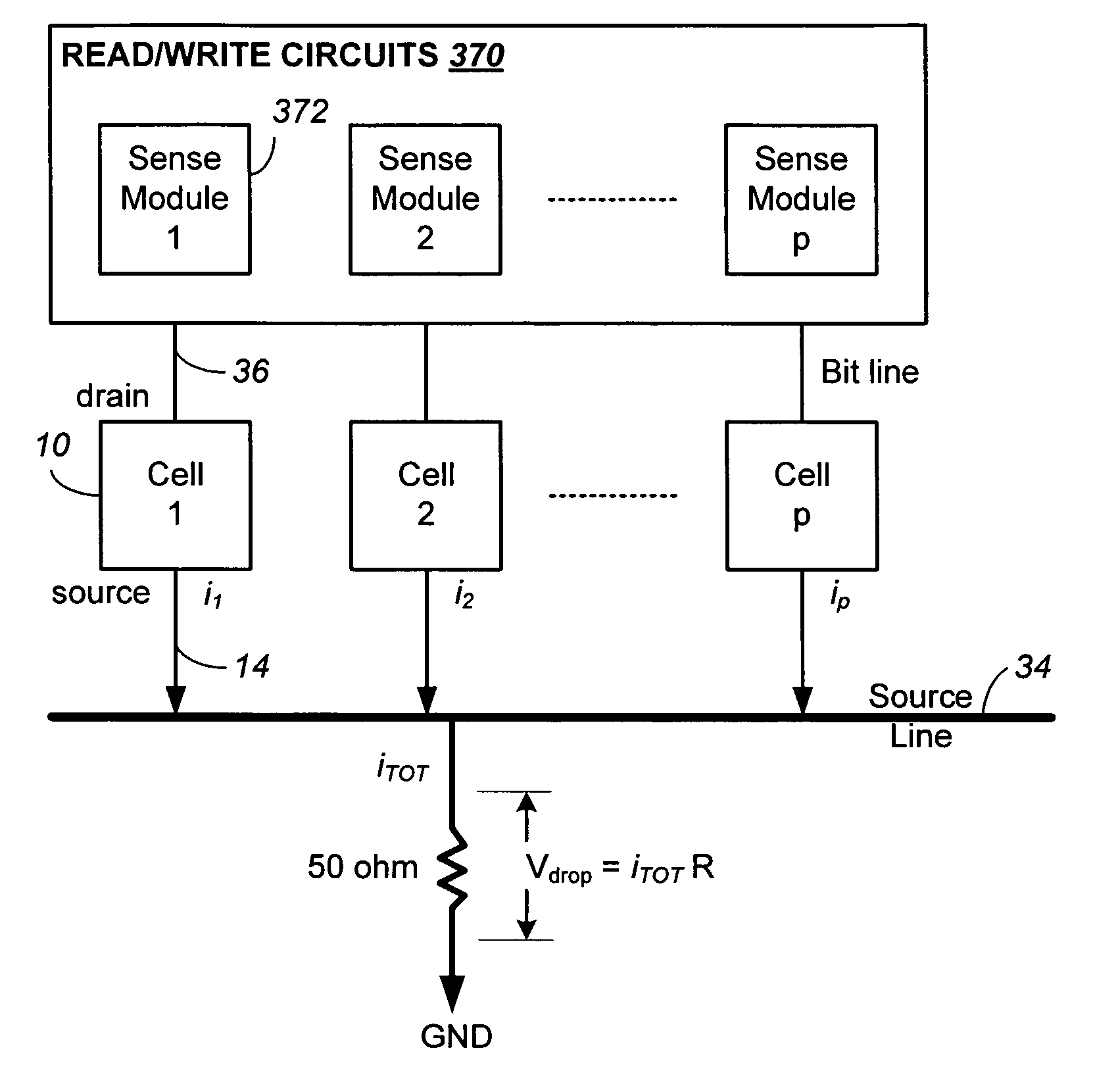
[0102]FIG. 6A illustrates schematically a memory device having read / write circuits for reading and programming a page of memory cells in parallel, according to one embodiment of the present invention. The memory device includes a two-dimensional array of memory cells 300, control circuitry 310, and read / write circuits 370. The memory array 300 is addressable by word lines via a row decoder 330 and by bit lines via a column decoder 360. The read / write circuits 370 include multiple sense modules 380 and allow a page of memory cells to be read or programmed in parallel. In one embodiment, where a row of memory cells are partitioned into multiple pages, a page multiplexer 350 is provided to multiplex the read / write circuits 370 to the individual pages.

[0103] The control circuitry 310 cooperates with the read / write circuits 370 to perform memory operations on the memory array 300. The control circuitry 310 includes a state machine 312, an on-chip address decoder 314 and a power control ...


PUM


Abstract

One or more sense amplifiers for sensing the conduction current of non-volatile memory is controlled by signals that are timed by a reference sense amplifier having similar characteristics and operating conditions. In one aspect, a sensing period is determined by when the reference sense amplifier sensing a reference current detects an expected state. In another aspect, an integration period for an amplified output is determined by when the reference sense amplifier outputs an expected state. When these determined timings are used to control the one or more sense amplifiers, environment and systemic variations are tracked.

Description

CROSS REFERENCE TO RELATED APPLICATIONS [0001] This application is a continuation-in-part of U.S. patent application Ser. No. 11 / 015,199 filed on Dec. 16, 2004, which is a continuation-in-part of U.S. patent application Ser. No. 10 / 665,828, filed on Sep. 17, 2003, which is a continuation-in-part of U.S. patent application Ser. No. 10 / 254,830, filed on Sep. 24, 2002. This application is related to U.S. patent application Ser. No. ______ filed concurrently entitled “Method for Compensated Sensing in Non-Volatile Memory”. These applications are incorporated herein in their entirety by this reference.FIELD OF THE INVENTION [0002] This invention relates generally to non-volatile semiconductor memory such as electrically erasable programmable read-only memory (EEPROM) and flash EEPROM, and specifically ones having improved sensing circuits that operate with a low voltage supply. BACKGROUND OF THE INVENTION [0003] Solid-state memory capable of nonvolatile storage of charge, particularly in...

Claims


Application Information

Patent Timeline
IPC IPC(8): G11C7/02G11C7/00G11C7/06G11C11/56G11C16/26G11C16/28
CPCG11C7/062G11C7/067G11C7/08G11C7/227G11C11/5628G11C11/5642G11C16/10G11C16/26G11C16/28G11C2211/5621G11C2216/14G11C2216/22G11C7/04
Inventor CHAN, SIU LUNGCERNEA, RAUL-ADRIAN
Owner SANDISK TECH LLC
Why Eureka
Try Eureka