

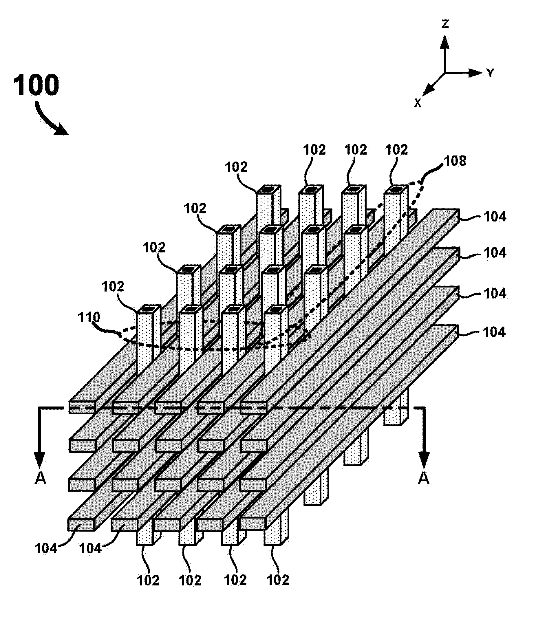
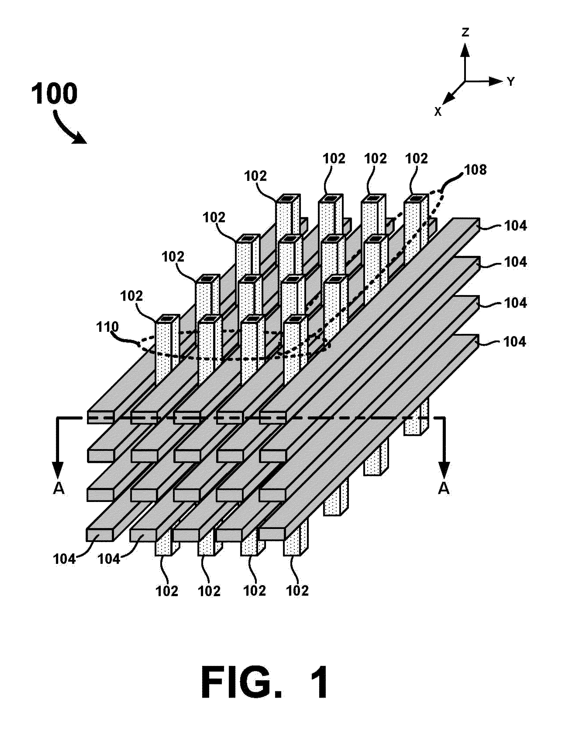
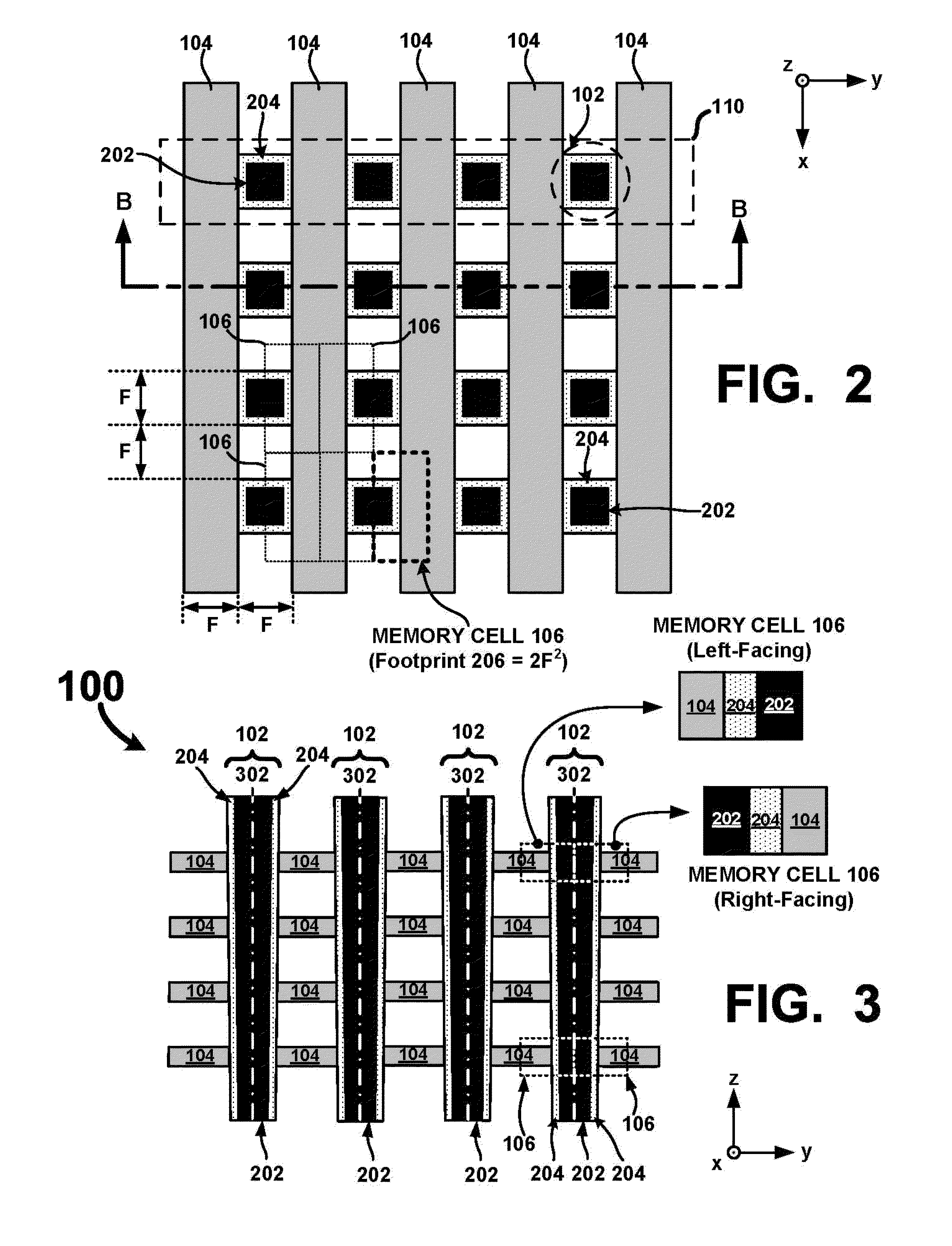
Vertical Cross Point Arrays For Ultra High Density Memory Applications
a memory array and vertical cross point technology, applied in the field of memory arrays, can solve the problems of diffraction limits, unable to scale down further, and various challenges to integrating memory cells in high-density memory arrays, and achieve the effect of increasing capacities
- Summary
- Abstract
- Description
- Claims
- Application Information
AI Technical Summary
Benefits of technology
Problems solved by technology
Method used
Image

Examples
Embodiment Construction
[0039]A detailed description of one or more examples is provided below along with accompanying figures. The detailed description is provided in connection with such examples, but is not limited to any particular example. The scope is limited only by the claims, and numerous alternatives, modifications, and equivalents are encompassed. Numerous specific details are set forth in the following description in order to provide a thorough understanding. These details are provided as examples and the described techniques may be practiced according to the claims without some or all of the accompanying details. For clarity, technical material that is known in the technical fields related to the examples has not been described in detail to avoid unnecessarily obscuring the description. The described fabrication techniques may be varied and are not limited to the examples provided.
[0040]Various embodiments or examples may be implemented in numerous ways, including as a system, a process, an ap...
PUM
 Abstract
Description
Claims
Application Information