Storage device and information processing system

Active Publication Date: 2006-04-27
SONY CORP
View PDF8 Cites 202 Cited by
  • Summary
  • Abstract
  • Description
  • Claims
  • Application Information

AI Technical Summary

Benefits of technology

[0086] Further, in the embodiment of the present invention, it is judged whether or not the desired data is present in the NVRAM by using an address conversion table. This provides the following flexibility to a general cache system using cache tags for judgment. In the usual cache system, only a copy of the data stored in the main memory is stored in the cache. Accordingly, when data in the cache is updated from the outside, it is necessary to write it back to the original position of the main memory without fail. As previously explained, when using the flash memory as

Problems solved by technology

However, as explained above, a flash memory has the defect that an increase of speed cannot be achieved unless the access unit is made large.
Further, data cannot be over

Method used


Image

  • Storage device and information processing system
  • Storage device and information processing system
  • Storage device and information processing system

Examples


first embodiment

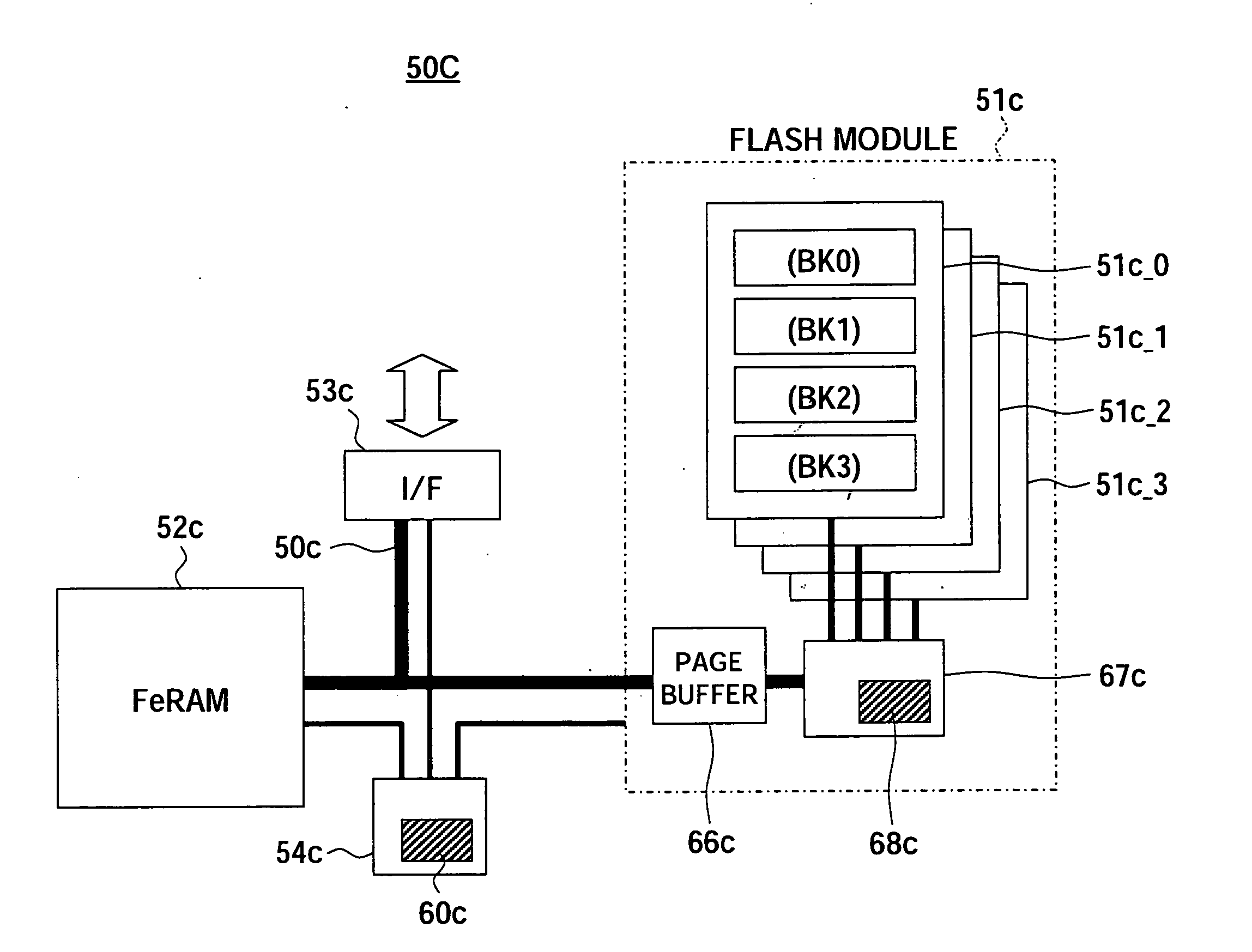
[0117]FIG. 6 is a view of the configuration of a storage device according to a first embodiment of the present invention.

[0118] A storage device 50 of FIG. 6 has, as principal components, a main memory 51, an auxiliary memory 52, an interface circuit (I / F) 53, a transfer control circuit 54, and an internal bus BS50.

[0119] That is, the storage device 50 is comprised of a large capacity main memory 51 configured by a NAND type flash memory and a relatively small capacity auxiliary memory 52 configured by a ferroelectric memory connected to an input / output interface circuit 53 with the outside via the internal bus BS50 and further has the transfer control circuit 54. The main memory 51 has an internal portion arranged in parallel at a high level, in which a group of data of 32 kB is simultaneously accessed as unit pages and input / output and transferred to the internal bus BS50.

[0120] Further, the device is formed with an address conversion table 60 using the above pages as managemen...

second embodiment

[0158]FIG. 11 is a view of the configuration showing a storage device according to a second embodiment of the present invention. A storage device 80 of the second embodiment is a storage device using a hard disk drive (HDD) as the main memory.

[0159] The storage device 80 of FIG. 11 has a main memory 81, an auxiliary memory 82, an interface circuit (I / F) 83, a transfer control circuit 84, and an internal bus BS80 as principal components.

[0160] The input / output interface circuit 83 with the outside is connected to a large capacity main memory 81 configured by a hard disk drive and a relatively small capacity auxiliary memory 82 configured by a ferroelectric memory via the internal bus BS80 and further has a transfer control circuit 84. According to the control signal from the transfer control circuit 84, the main memory 81 and the auxiliary memory 82 transfer data in two ways in the data group in units of for example 32 kB (hereinafter referred to as a “page”). Further, the data is ...

third embodiment

[0170] Even when apply part of the concept of the present invention to an existing cache memory system, it is possible to obtain similar effects. An explanation will be given of the configuration of a storage device managing an auxiliary memory as a cache memory as a third embodiment for a system the same as that of the embodiment of FIG. 6.

[0171]FIG. 13 is a view of the configuration of a storage device according to a third embodiment of the present invention.

[0172] A storage device 50B of FIG. 13 has a main memory 51b, an auxiliary memory 52d, an interface circuit (I / F) 53b, a transfer control circuit 54b, and an internal bus BS50b as the principal components.

[0173] In such a memory system, a page table 60b is used for only management of the main memory 51b. The physical address covers only the region on the main memory 51b side. On the other hand, the content on the auxiliary memory side is managed by separately providing an entry table 63b of the cache as shown in FIG. 13 and...


PUM


Abstract

A storage device able to make a redundant write operation of unselected data unnecessary and able to optimize an arrangement of pages to a state having a high efficiency for rewriting, wherein the storage device has a first memory unit, a second memory unit having a different access speed from the first memory, and a control circuit, wherein the control circuit has a function of timely moving the stored data in two ways between the first memory unit and the second memory unit having different access speeds in reading or rewriting.

Description

CROSS REFERENCES TO RELATED APPLICATIONS [0001] The present invention contains subject matter related to Japanese Patent Application No. 2004-312500 filed in the Japan Patent Office (JPO) on Oct. 27, 2004, Japanese Patent Application No. 2004-312501 filed in the JPO on Oct. 27, 2004, Japanese Patent Application No. 2005-018370 filed in the JPO on Jan. 26, 2005, and Japanese Patent Application No. 2005-171141 filed in the JPO on Jun. 10, 2005, the entire contents of which being incorporated herein by reference. BACKGROUND OF THE INVENTION [0002] 1. Field of the Invention [0003] The present invention relates to a storage device including a non-volatile memory and an information processing system, more particularly relates to speedup of data transfer in a storage device including a flash memory. [0004] 2. Description of the Related Art [0005] In recent years, as a storage medium of a digital still camera or mobile computer device, attention is paid to a flash memory. [0006] A flash mem...

Claims


Application Information

Patent Timeline
IPC IPC(8): G11C7/10
CPCG06F12/0246G06F12/08G06F12/0866G06F2212/2022G11C8/08G11C11/22Y02B60/1225G06F12/00G06F12/0813G06F12/1081G06F13/28G06F2212/1024G06F2212/7201G06F2212/2024Y02D10/00G11C16/00G06F3/0641G06F12/0223G06F12/10G06F12/1009
Inventor NISHIHARA, TOSHIYUKISAKAI, YOSHIO
Owner SONY CORP
Why Eureka
Try Eureka