Plasma display device

A technology for plasma display panels and display devices, which is applied to identification devices, static indicators, cathode ray tube indicators, etc., can solve the problems of limited number of pixels, reduced image expressiveness, and increased manufacturing unit price of plasma display panels, etc. The effect of reducing the manufacturing unit price and improving the expressiveness

Inactive Publication Date: 2007-07-18
LG ELECTRONICS(NANJING) PLASMA CO LTD
View PDF0 Cites 11 Cited by
  • Summary
  • Abstract
  • Description
  • Claims
  • Application Information

AI Technical Summary

Problems solved by technology

[0012] Therefore, the number of pixels that can be formed on a certain area of ​​the plasma display panel is limited, and thus there is a problem that image expression is reduced
[0013] Moreover, in

Method used


Image

  • Plasma display device
  • Plasma display device
  • Plasma display device

Examples


Embodiment Construction

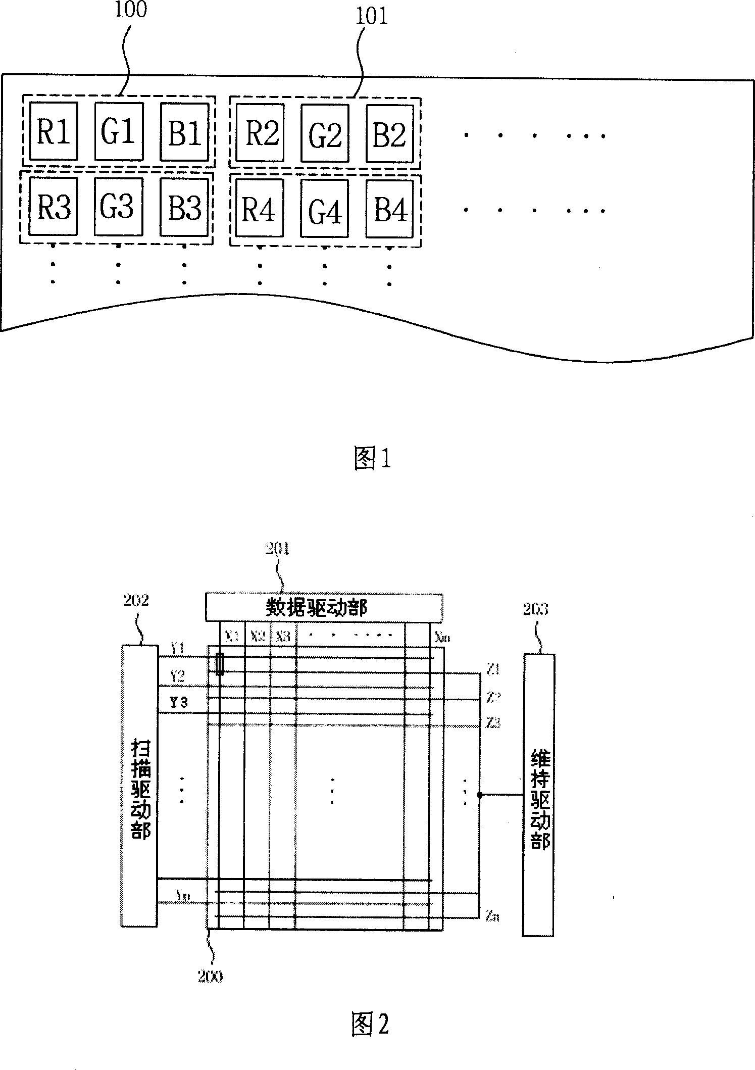
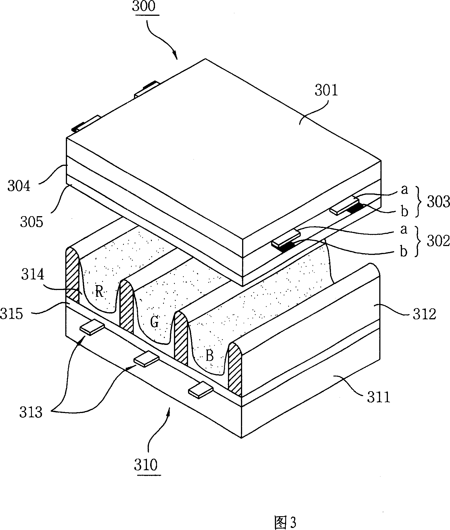
[0038] Hereinafter, the plasma display device of the present invention will be described in detail with reference to the attached pictures.

[0039] FIG. 2 is a diagram illustrating a plasma display device of the present invention.

[0040] Analyzing FIG. 2 , the plasma display device of the present invention includes a plasma display panel 200 , a data drive unit 201 , a scan drive unit 202 , and a sustain drive unit 203 .

[0041] Wherein, in the plasma display panel 200, a front substrate (not shown in the figure) and a rear substrate (not shown in the figure) are bonded at certain intervals to form a plurality of electrodes. For example, scan electrodes Y and sustain electrodes Z aligned in the same direction as these scan electrodes Y are formed, and data electrodes X intersecting these scan electrodes Y and sustain electrodes Z are formed. Among them, a sub-pixel (Sub-Pixel) is formed at a point where the scan electrode Y, the sustain electrode Z, and the data electrode...


PUM


Abstract

A plasma display unit consists of plasma display plate formed by the first pixel including multiple sub-pixel and the second pixel sharing at least one sub-pixel with the first pixel, driving unit for providing certain signals to the first pixel and the second pixel and for carrying out scanning.

Description

technical field [0001] The present invention is an invention related to a plasma display panel, more specifically, an invention related to a plasma display device that improves the arrangement structure of a plurality of sub-pixels. Background technique [0002] Usually, a plasma display panel consists of a barrier formed between the front substrate and the rear substrate to form a sub-pixel (Sub-Pixel), and the sub-pixel is filled with neon (Ne), helium (He) or a mixed gas containing neon and helium ( Ne+He) and a small amount of xenon (Xe) discharge gas. These sub-pixels constitute a plurality of pixels (Pixels) for displaying images. For example, red (Red, R), green (Green, G), and blue (Blue, B) sub-pixels are combined into one pixel. [0003] Moreover, when the plasma display panel is discharged by a high-frequency voltage, the discharge gas generates vacuum ultraviolet rays (Vacuum Ultraviolet rays), which makes the phosphors formed between the barrier ribs emit ligh...

Claims


Application Information

Patent Timeline
IPC IPC(8): G09G3/28G09G3/20G09G5/02H01J17/49G09F9/313G09G3/288
Inventor 柳聖煥
Owner LG ELECTRONICS(NANJING) PLASMA CO LTD
Why Eureka
Try Eureka