Border scanning test structure of multiple chip package internal connection and test method

A boundary scan test, multi-chip packaging technology, applied in the direction of semiconductor/solid-state device test/measurement, single semiconductor device test, etc., can solve the problems of connection between chips, shorten the time to use, shorten the test time, and reduce the number of chips The effect of time and steps of program writing

Active Publication Date: 2007-11-28
RDA MICROELECTRONICS SHANGHAICO LTD
View PDF9 Cites 29 Cited by
  • Summary
  • Abstract
  • Description
  • Claims
  • Application Information

AI Technical Summary

Problems solved by technology

The above circuit structure can not only solve the problem of connecting chips in the package, but also realize the programming of programmable devices in the package through the mechanism of JTAG and boundary scan.

Method used


Image

  • Border scanning test structure of multiple chip package internal connection and test method
  • Border scanning test structure of multiple chip package internal connection and test method
  • Border scanning test structure of multiple chip package internal connection and test method

Examples


Embodiment Construction

[0036] The present invention will be further described below in conjunction with the accompanying drawings and specific embodiments.

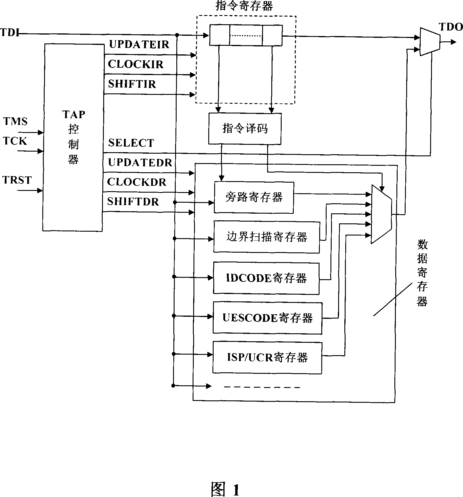
[0037] Figure 1 is a typical boundary scan test circuit structure diagram. However, under the requirements of the special products targeted by the present invention, that is, the number of chips in the package is large, the connection relationship is complicated, and the number of pins connected to the outside of the package is extremely limited. For example, in smart card products, there are only 8 external connection pins. The traditional 4 (or 5) boundary scan dedicated test pins TDI, TDO, TCK, TMS and TRST (optional pins) on the chip in the package cannot be directly connected to the outside of the package.

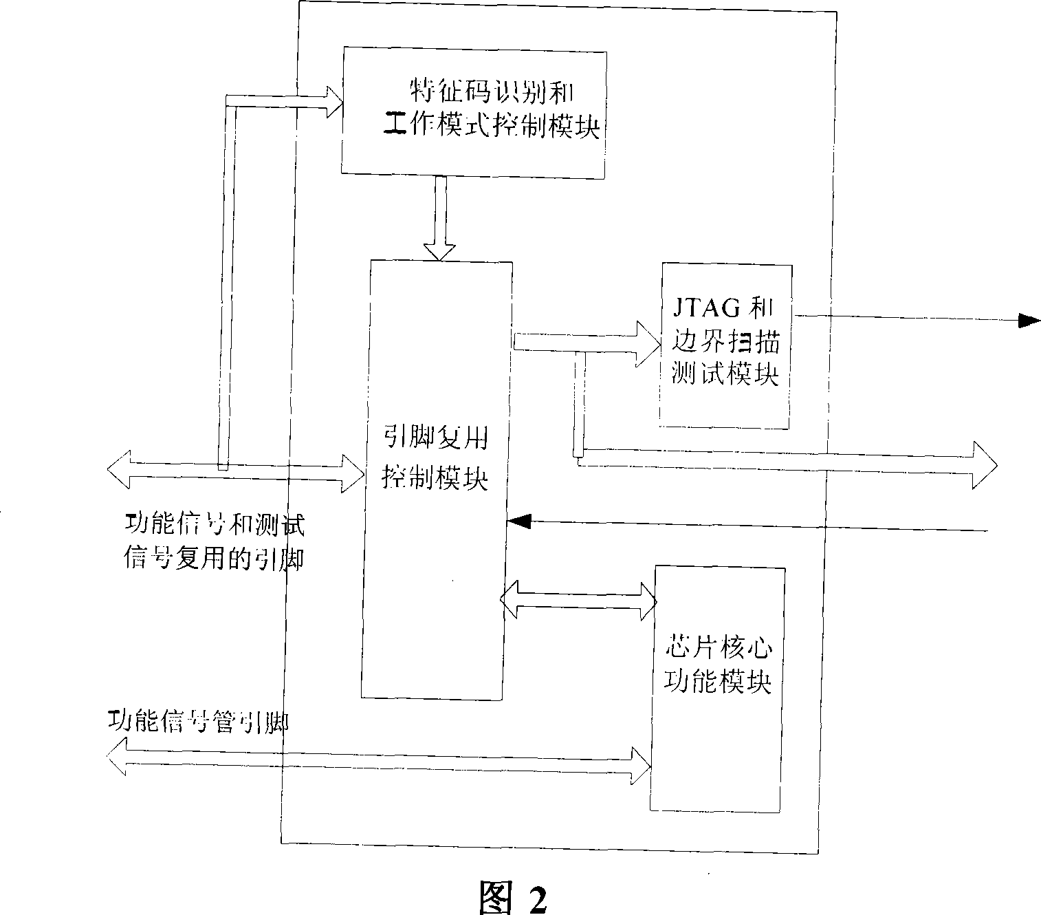
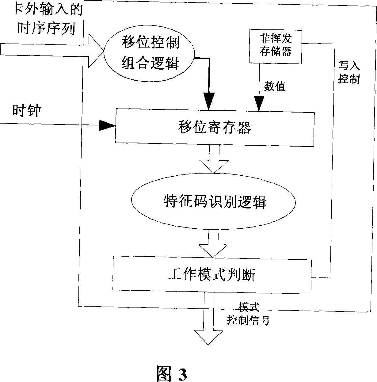
[0038] Figure 2 shows a solution under the special complex conditions mentioned above. The five pins required for JTAG and boundary scan will be multiplexed with the normal operating signal pins of the package when the circuit is impl...


PUM


Abstract

The invention relates to a boundary scanning testing structure connected with multiple-chip packaging body with finite pins in it and the testing method, belonging to IC chip design, chip testability design and chip packaging fields. A typical application is the modern new SIM card with large capacity constituted by multiple chips. The invention sets finite functional pins of packaging body as pins with boundary scanning function by a special logic sequence relationship when multiple-chip packaging body is tested and then by these pins boundary scanning test in packaging body can be carried out so as to achieve the test to inner connection relationship of packaging body. After test is done, by a special operation, the function of testing circuit is closed to avoid chip error action, which is not necessary in future. The invention realizes special power-on flow of chip, realization of a special circuit and corresponding structure adjustment of chip.

Description

technical field [0001] The invention belongs to the technical fields of integrated circuit chip design, chip testability design, and chip packaging, and specifically relates to a test circuit structure and a test method, which are used to realize the large number of internal chips and the number of pins connected to each other in multi-chip packaging. In the case that there are many, the connection relationship is complicated, and the number of external connection pins of the final package body is very small, the connection relationship in the package body is tested after the packaging process is completed. Background technique [0002] With the development of modern electronics industry, the complexity of electronic circuit boards is increasing day by day. This complexity is reflected in the increase in the number of components on the same PCB and the increase in the complexity of the interconnection between components. This brings great challenges to the inspection of the...

Claims


Application Information

Patent Timeline
Patent Type & Authority Applications(China)
IPC IPC(8): G01R31/26H01L21/66
Inventor 支军卜冀春詹志勇
Owner RDA MICROELECTRONICS SHANGHAICO LTD
Why Eureka
Try Eureka