Eureka AIR delivers breakthrough ideas for toughest innovation challenges, trusted by R&D personnel around the world.

Fixation carrier, production method of fixation carrier, use method of fixation carrier, and substrate reception container

A technology for fixing carriers and manufacturing methods, applied in semiconductor/solid-state device manufacturing, electrical components, circuits, etc., can solve problems such as bad conditions, easy warping, and easy breakage, and achieve the effect of preventing damage

Inactive Publication Date: 2011-08-17
SHIN-ETSU POLYMER CO LTD
View PDF1 Cites 1 Cited by
  • Summary
  • Abstract
  • Description
  • Claims
  • Application Information

AI Technical Summary

Problems solved by technology

[0005] Conventional semiconductor wafers are processed as above, and become very thin by back grinding, and tend to warp and break easily, so there is a big problem that it is difficult to properly transport from the factory to other factories without being damaged.
[0006] As a method to solve this problem, the method of using the above-mentioned dedicated carrier is considered, but this carrier is only a special product used in the transportation in the factory, and it is not a structure that takes into account the harsh transportation conditions, so it cannot be transferred from the factory to the carrier. Used for long-term transportation in factories
[0007] In addition, when the dicing tape is attached to the semiconductor wafer for a long time during transportation from factory to factory, the adhesive of the dicing tape may be transferred to the bumps of the circuit, causing a problem.

Method used


Image

  • Fixation carrier, production method of fixation carrier, use method of fixation carrier, and substrate reception container
  • Fixation carrier, production method of fixation carrier, use method of fixation carrier, and substrate reception container
  • Fixation carrier, production method of fixation carrier, use method of fixation carrier, and substrate reception container

Examples


Embodiment Construction

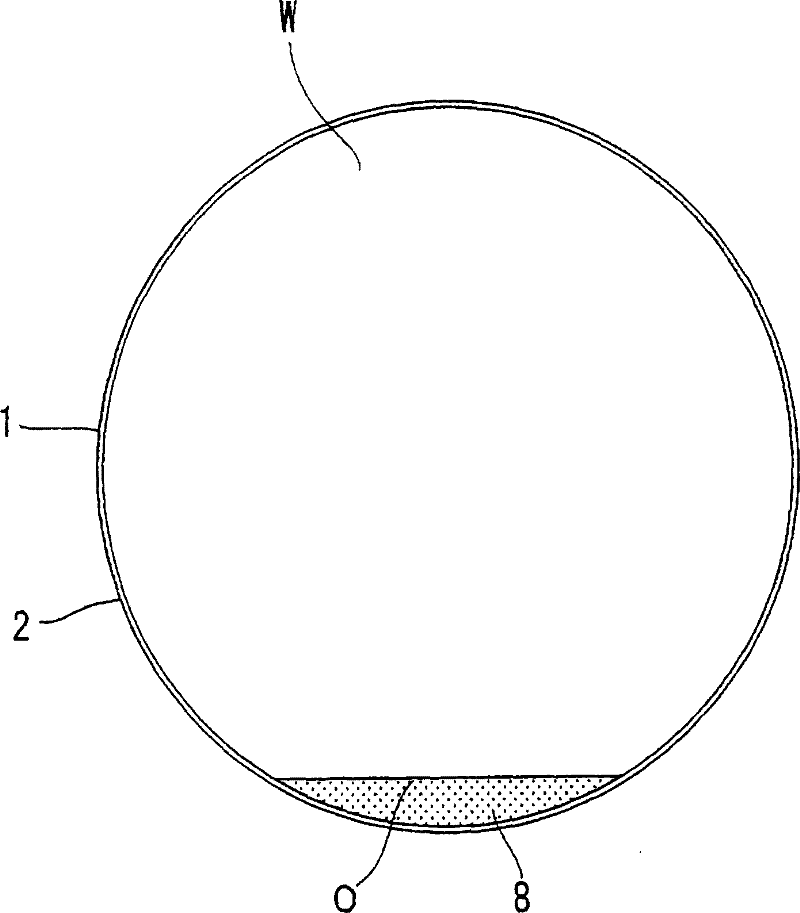
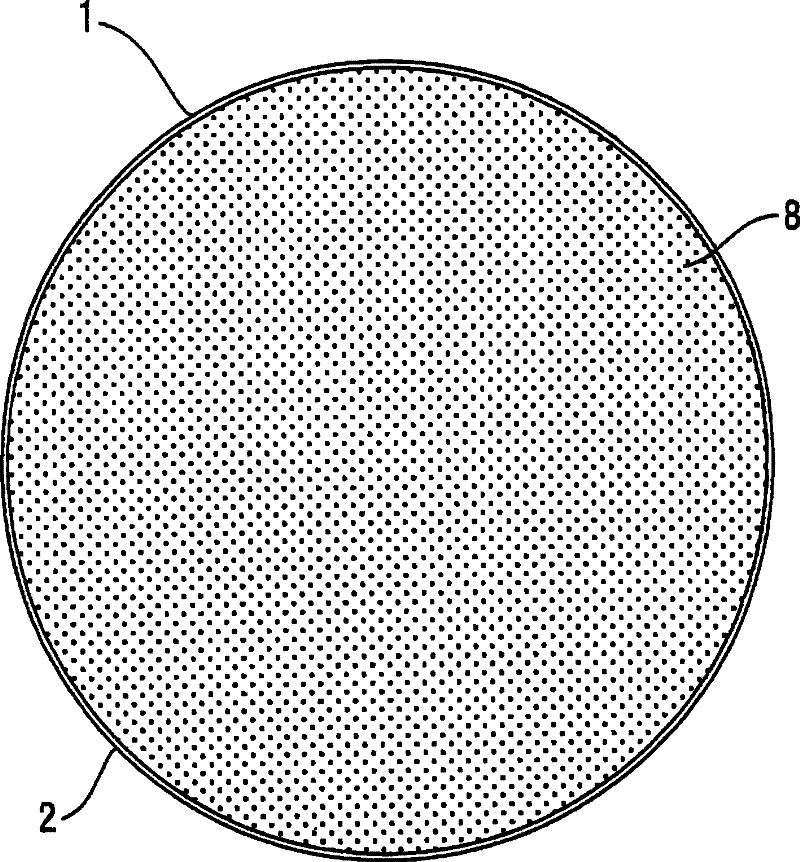
[0084] Hereinafter, preferred embodiments of the present invention will be described with reference to the accompanying drawings, and the fixed carrier 1 of the present embodiment is as follows: Figure 1 to Figure 15 As shown, it is equipped with a rigid base material 2 and an elastically deformable holding layer 8 covering the base material 2 to hold a semiconductor wafer W with a diameter of 300 mm (12 inches). container 20.

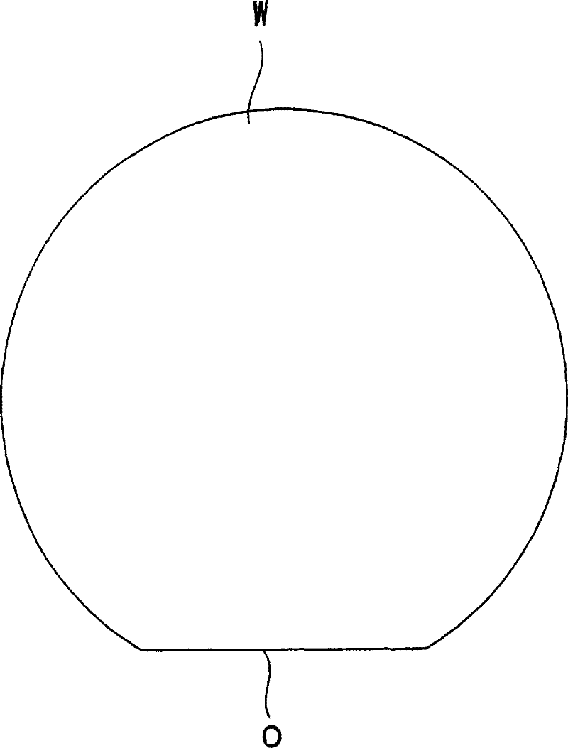
[0085] Semiconductor wafer W such as figure 1 and figure 2 As shown, it is basically composed of a round silicon wafer with a thickness of about 750 μm, and a linear orientation flat O (orientation flat) or a notch N is notched on the peripheral portion, and the orientation flat O or notch N is used to determine the crystal orientation and function for positioning. The semiconductor wafer W is bonded with a protective tape on the surface of the mirror surface on which the circuit is formed as a pattern, and the back surface is ground by a back gri...


PUM


Abstract

An object is to provide a fixing carrier, a fixing carrier manufacturing method, a method of using the fixing carrier and a substrate storage container, which provide proper shipment of items to be loaded that are prone to warp and crack. A base 2 having rigidity is hollowed on its surface and formed with a sectioned space 3 laminated and covered by a supporting layer 8 that supports semiconductor wafer W, multiple projections 4 that are formed in the sectioned space and supports supporting layer 8 in contact therewith and an exhaust passage 6 that is bored through base 2 and draws air out ofsectioned space 3 covered by supporting layer 8. Since semiconductor wafer W that is prone to warp and crack is supported by supporting layer 8 of a fixing carrier 1 and accommodated in the containerbody of a substrate storage container, instead of being kept directly in the container, so it is possible to achieve safe and proper shipment between factories.

Description

technical field [0001] The present invention relates to a fixed carrier for mounted articles composed of substrates represented by semiconductor wafers, quartz glass, etc., printed wiring boards, chip components, and other components that are difficult to hold individually, a method of manufacturing a fixed carrier, and use of a fixed carrier Method and substrate storage container. Background technique [0002] In recent years, the diameter of semiconductor wafers has been expanded from 200mm to 300mm. After the circuit is patterned and formed on the surface of this 300mm type semiconductor wafer, in view of the packaging requirements of the laminated structure, etc., a protective tape for backside grinding is attached to the surface, and The back surface of the back surface is ground and thinned by a back grinding device, then supplied to a slicing process, the protective tape is peeled off, and a slicing tape for the slicing process is attached. [0003] The semiconductor...

Claims


Application Information

Patent Timeline
Patent Type & Authority Patents(China)
IPC IPC(8): H01L21/673
CPCH01L21/67383H01L21/67346H01L21/67393H01L21/68H01L21/67
Inventor 小田岛智细野则义
Owner SHIN-ETSU POLYMER CO LTD
Why Eureka
Eureka Blog
Learn More