Ganged scanning of multiple magnetrons, especially two level folded magnetrons

A magnetron and linkage technology, applied in the field of magnetron, can solve problems such as incomplete target utilization

Active Publication Date: 2012-09-19
APPLIED MATERIALS INC
View PDF5 Cites 0 Cited by
  • Summary
  • Abstract
  • Description
  • Claims
  • Application Information

AI Technical Summary

Problems solved by technology

[0010] However, previously available magnetron sputtering chambers for large flat panels have shown incomplete target utilization

Method used


Image

  • Ganged scanning of multiple magnetrons, especially two level folded magnetrons
  • Ganged scanning of multiple magnetrons, especially two level folded magnetrons
  • Ganged scanning of multiple magnetrons, especially two level folded magnetrons

Examples


Embodiment Construction

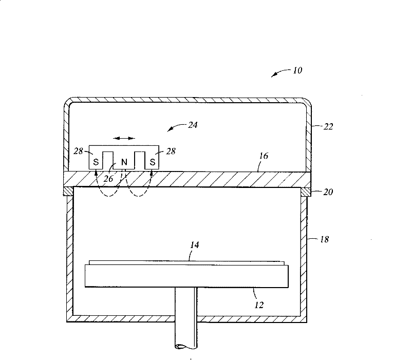
[0029] One embodiment of the source assembly of the present invention separates both the target and the magnetron into associated bar targets and bar magnetrons. The bar targets are supported on a separate target holder and the bar magnetrons are supported on a separate scanning support plate so that the magnetrons are linked during scanning.

[0030] Another embodiment includes a magnetron suitable for use in a ganged magnetron assembly or other magnetron configuration.

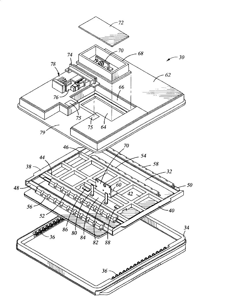
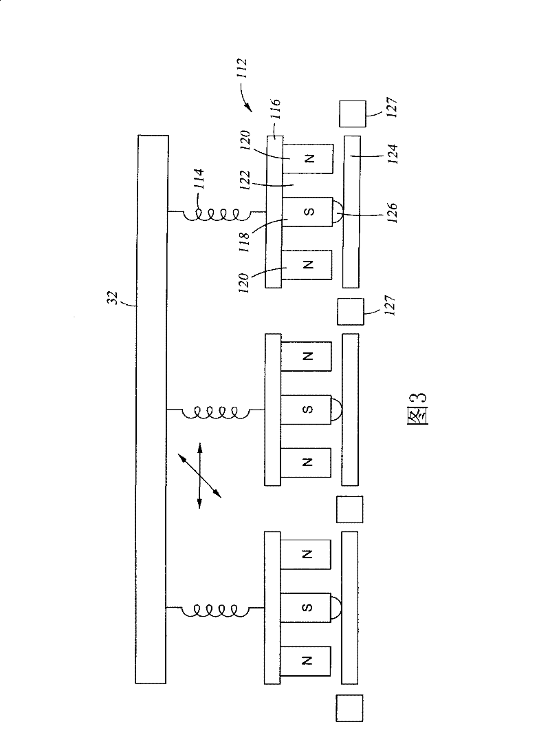
[0031] exist figure 2 The two-dimensional scanning mechanism 30 shown in the orthogonal view is close to the scanning mechanism described by Le et al. Submitted applications should be considered in more detail. However, the scanning mechanism 30 supports a large support plate 32 that is preferably composed of a non-magnetic material such as aluminum, and the scanning mechanism 30 can scan the large support plate 32 in an arbitrary two-dimensional pattern. In contrast, Tepman and Le's setup scans a single...


PUM


Abstract

A magnetron assembly including one or more magnetrons each forming a closed plasma loop on the sputtering face of the target. The target may include multiple strip targets on which respective strip magnetrons roll and are partially supported on a common support plate through a spring mechanism. The strip magnetron may be a two-level folded magnetron in which each magnetron forms a folded plasma loop extending between lateral sides of the strip target and its ends meet in the middle of the target. The magnets forming the magnetron may be arranged in a pattern having generally uniform straight portions joined by curved portion in which extra magnet positions are available near the corners to steer the plasma track. Multiple magnetrons, possibly flexible, may be resiliently supported on a scanned support plate and individually partially supported by rollers on the back of one or more targets.

Description

[0001] This application claims priority to provisional applications 60 / 835,671 and 60 / 835,681, filed August 4,2006. This application is also related to Serial No. 11 / 601,576, filed November 17, 2006. technical field [0002] The present invention relates generally to sputter deposition in the manufacture of semiconductor integrated circuits. In particular, the present invention relates to magnetrons that scan across the backside of a plasma sputtering target. Background technique [0003] Plasma magnetron sputtering has been practiced for a long time in the fabrication of silicon integrated circuits. More recently, sputtering has been applied to deposit layers of material on large and often discrete rectangular plates of glass, metal or polymers, or equivalent sheets. The completed panel may comprise thin film transistors, plasma displays, field emitters, liquid crystal display (LCD) elements or organic light emitting diodes (OLEDs) and typically involves flat panel displa...

Claims


Application Information

Patent Timeline
Patent Type & Authority Patents(China)
IPC IPC(8): C23C14/35H01L21/203H01J37/34
CPCC23C14/3407C23C14/35H01J37/3266H01J37/3408H01J37/3455
Inventor 马裤托·艾娜加沃西门·明·胡·李阿基海伦·豪索卡沃布拉德利·O·斯廷森约翰·M·怀特
Owner APPLIED MATERIALS INC
Why Eureka
Try Eureka