Image sensor and image read device

An image sensor and imaging optics technology, applied in image communication, electrical components, etc., can solve the problems of deterioration of light receiving accuracy, weak intensity, and inability to prevent ghosting, etc., to achieve the effect of easy positioning adjustment, preventing random reflection, and improving light receiving accuracy.

Inactive Publication Date: 2008-06-04
NIPPON SHEET GLASS CO LTD
View PDF1 Cites 3 Cited by
  • Summary
  • Abstract
  • Description
  • Claims
  • Application Information

AI Technical Summary

Problems solved by technology

[0022] For example, when a hood with a slit is produced by resin injection molding, etc., since the strength of the resin molded product to maintain its own shape is weak, the accuracy of light reception deteriorates, and ghosting cannot be prevented at all positions in the longitudinal direction of the lens.

Method used


Image

  • Image sensor and image read device
  • Image sensor and image read device
  • Image sensor and image read device

Examples


Embodiment Construction

[0151] Next, the present invention will be specifically described.

[0152] (A) First, the case where the image sensor substrate is miniaturized will be described.

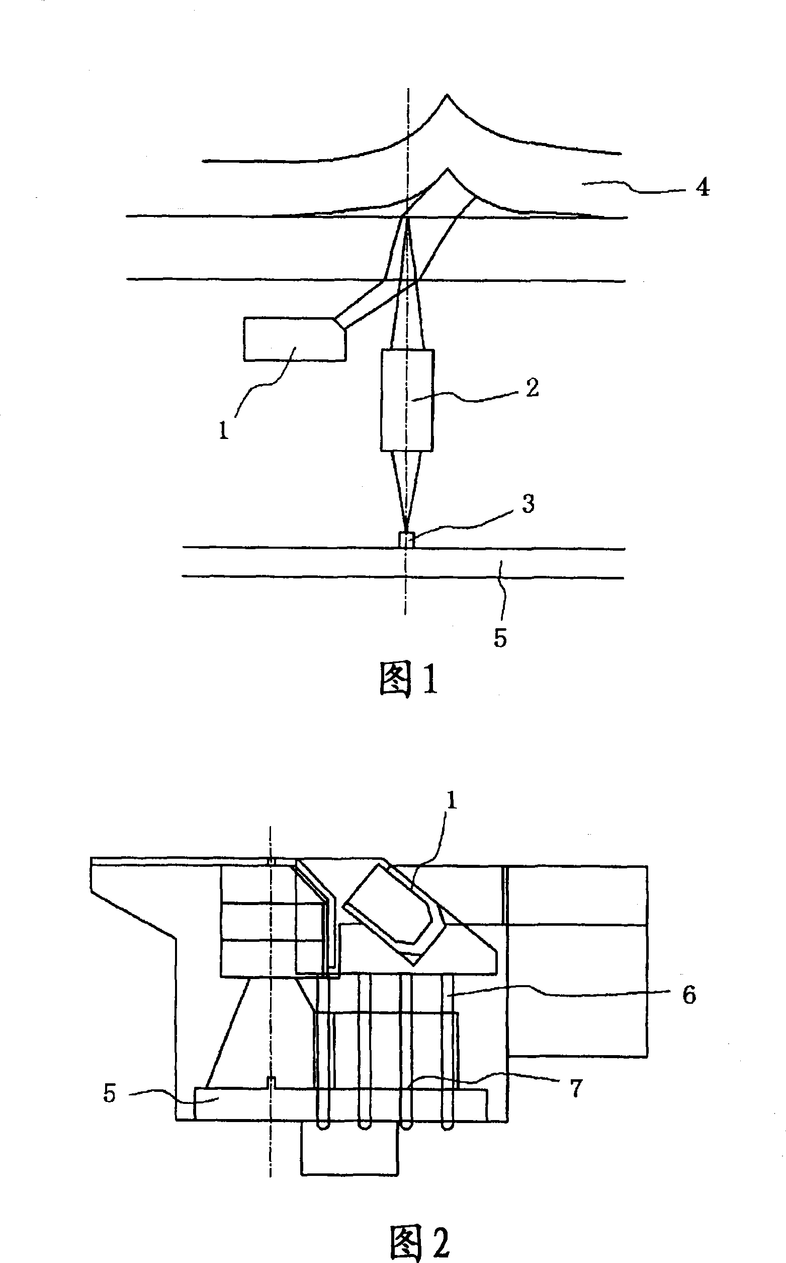
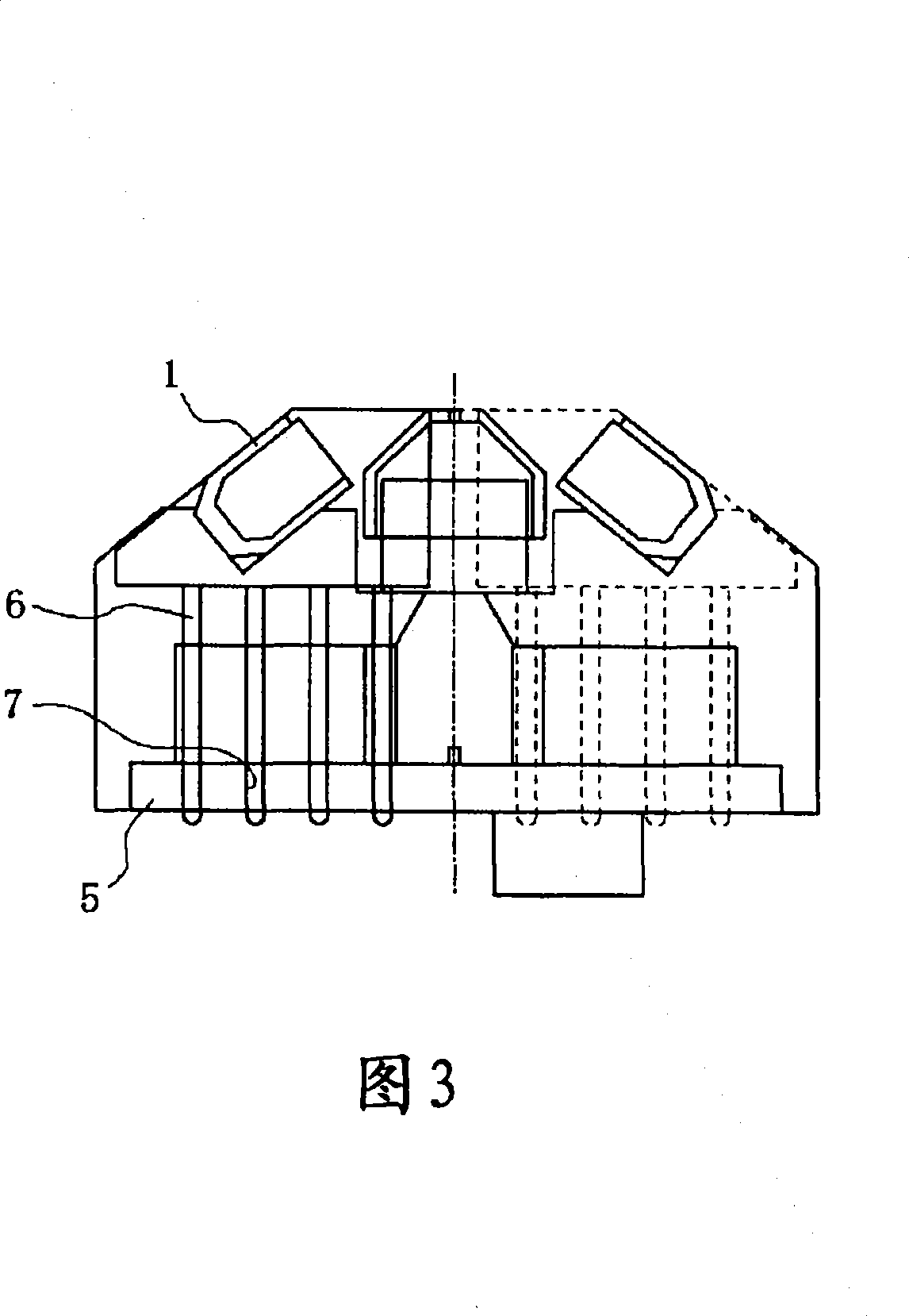
[0153] In addition, at this time, as shown in FIG. 5 , the terminal shape of the lead frame 6 of the rod-shaped light source 1 is changed.

[0154] That is, by bending the terminal of the lead frame 6 of the rod-shaped light source 1 toward the center side (center line side) of the substrate, the position of the through hole 7 in the substrate 5 is moved to the central portion, so that the position of the through hole 7 of the substrate 5 is positioned at the center of the substrate 5. Around the center.

[0155] According to the above configuration, as can be seen from a comparison with FIG. 3 , reduction in substrate width can be achieved.

[0156] The above describes the case where the rod light sources are arranged on both sides of the resin lens plate, but the present invention is not limited thereto, and t...


PUM


Abstract

The invention provides an image sensor and an image reading device. The image sensor does not require a significant increase of a substrate width even when a bar-shaped light source is arranged at both sides of a resin lens plate and having an excellent part positioning accuracy. The image sensor includes a bar-shaped light source for emitting light to an image to be read, an image formation optical system for collecting light reflected from the image to be read, and a light reception element for receiving light which has passed through the image formation optical system. The light reception element is arranged at a predetermined position of a substrate. The substrate has a through hole for receiving the terminal of a lead frame of the bar-shaped light source. The terminal of the lead frame of the bar-shaped light source is bent toward the center of the substrate and connected to the through hole.

Description

technical field [0001] The present invention relates to an image sensor and an image reading device including the image sensor, and particularly aims at reducing the size of an image sensor substrate. [0002] In addition, the present invention can effectively prevent ghosting and blurring, which are problems in an imaging optical system mounted on a unit for a writing optical system such as an optical printer or a reading optical system such as a scanner. [0003] Furthermore, the present invention seeks to advantageously improve the accuracy of the position of the slit with respect to the optical axis and the accuracy of the distance between the reading optical system and the document table. Background technique [0004] Image sensors are mounted on units for writing optical systems such as optical printers and reading optical systems such as scanners. [0005] A close-contact image sensor (contact image sensor), as shown in FIG. Take an image) 4, and detect the light re...

Claims


Application Information

Patent Timeline
IPC IPC(8): H04N1/028
Inventor 胁坂政英吉田治信
Owner NIPPON SHEET GLASS CO LTD
Why Eureka
Try Eureka