Chopper regulator circuit
A regulator circuit and voltage technology, applied in the direction of instruments, electric light sources, electrical components, etc., can solve the problems of increasing the total number, hindering the miniaturization and cost reduction of chopper regulator devices
- Summary
- Abstract
- Description
- Claims
- Application Information
AI Technical Summary
Problems solved by technology
Method used
Image
Examples
Embodiment 1
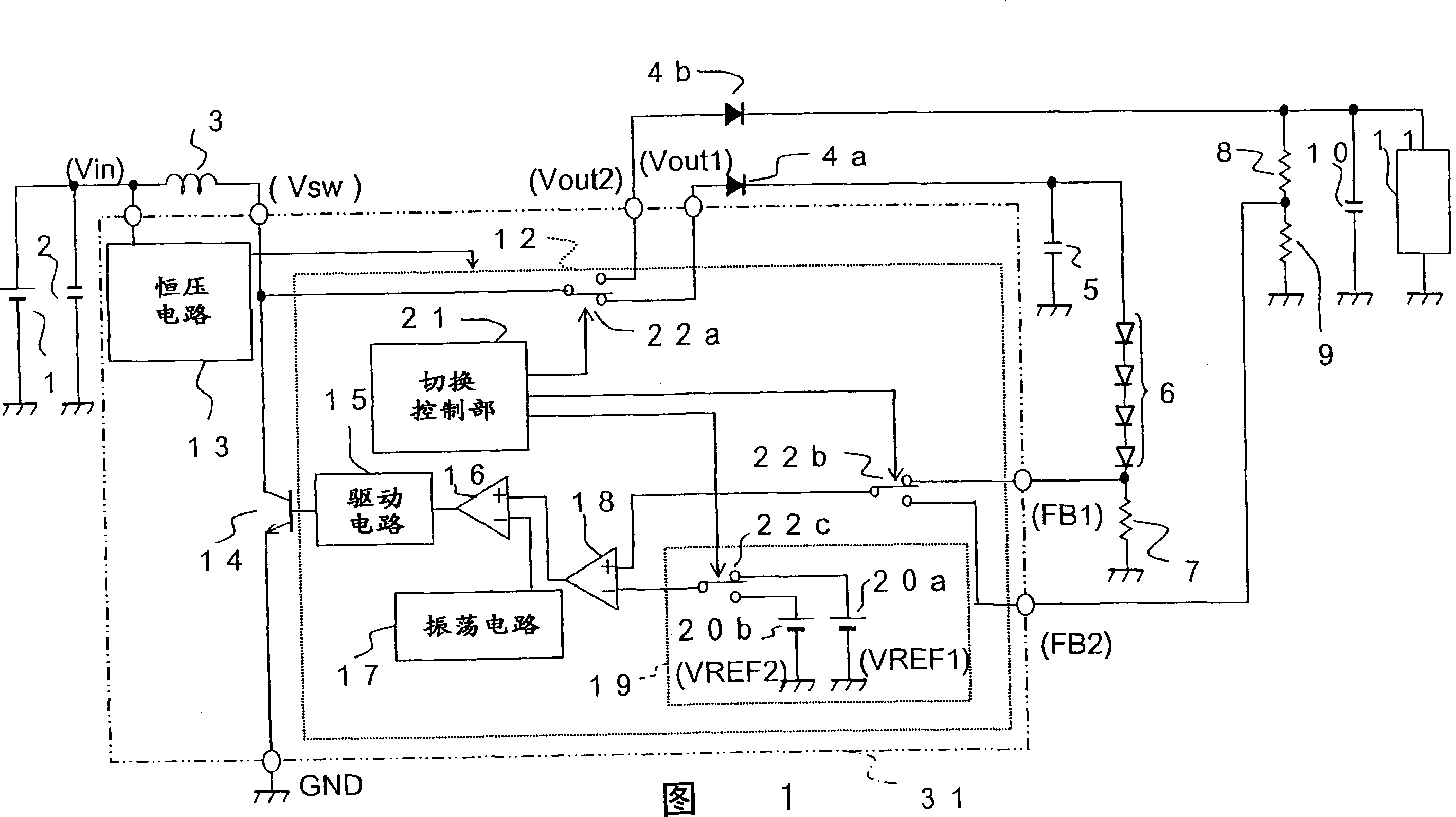
[0056] Embodiment 1: As a first embodiment of the present invention, a chopper connected to an LED group (which may be a single LED or a plurality of LEDs connected in series) and an organic EL element to selectively supply power to one of them will be described below. Regulator type power supply circuit. The configuration of this power supply circuit is shown in FIG. 1 .
[0057] As shown in FIG. 1, the power supply circuit includes a DC (direct current) power supply 1, an input capacitor 2, a coil 3, a first diode 4a, a second diode 4b, a first output capacitor 5, resistors 7 to 9, a first Two output capacitors 10, chopper regulator IC 31 and other components. Constructed as shown in FIG. 1 , the power supply circuit supplies electric power to the LED group 6 and the organic EL element 11 .
[0058] The negative terminal of the DC power supply 1 is grounded, while the positive terminal of the DC power supply 1 is connected to one end of the input capacitor 2 and one end of...
Embodiment 2
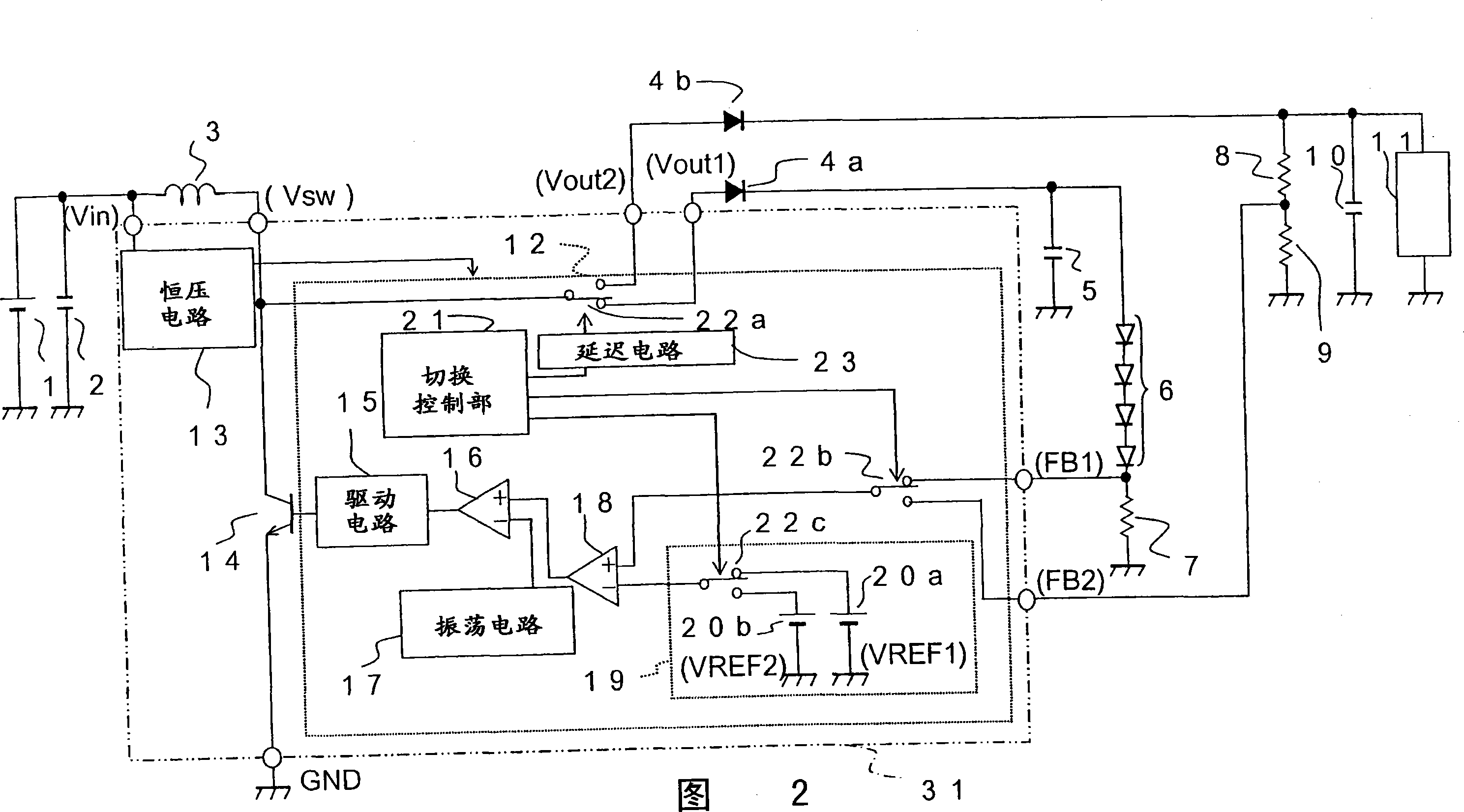
[0080] Embodiment 2: Next, as a second embodiment of the present invention, a power supply circuit will be described again below. The configuration here is largely the same as in Embodiment 1, the main difference being that a delay circuit is additionally provided. Therefore, overlapping descriptions will not be repeated.
[0081] FIG. 2 shows the configuration of the power supply circuit of this embodiment. As shown in the figure, in the chopper regulator IC 31, a delay circuit 23 is additionally provided between the switching control section 21 and the first switch 22a. The delay circuit 23 delays the switching signal output from the switching control section 21 by a predetermined time length to control switching of the first switch 22a, and then feeds the delayed switching signal to the first switch 22a.
[0082] Due to the delay circuit 23, even when the switching control section 21 outputs switching signals for switching the first to third switches 22a to 22c at the sam...
Embodiment 3
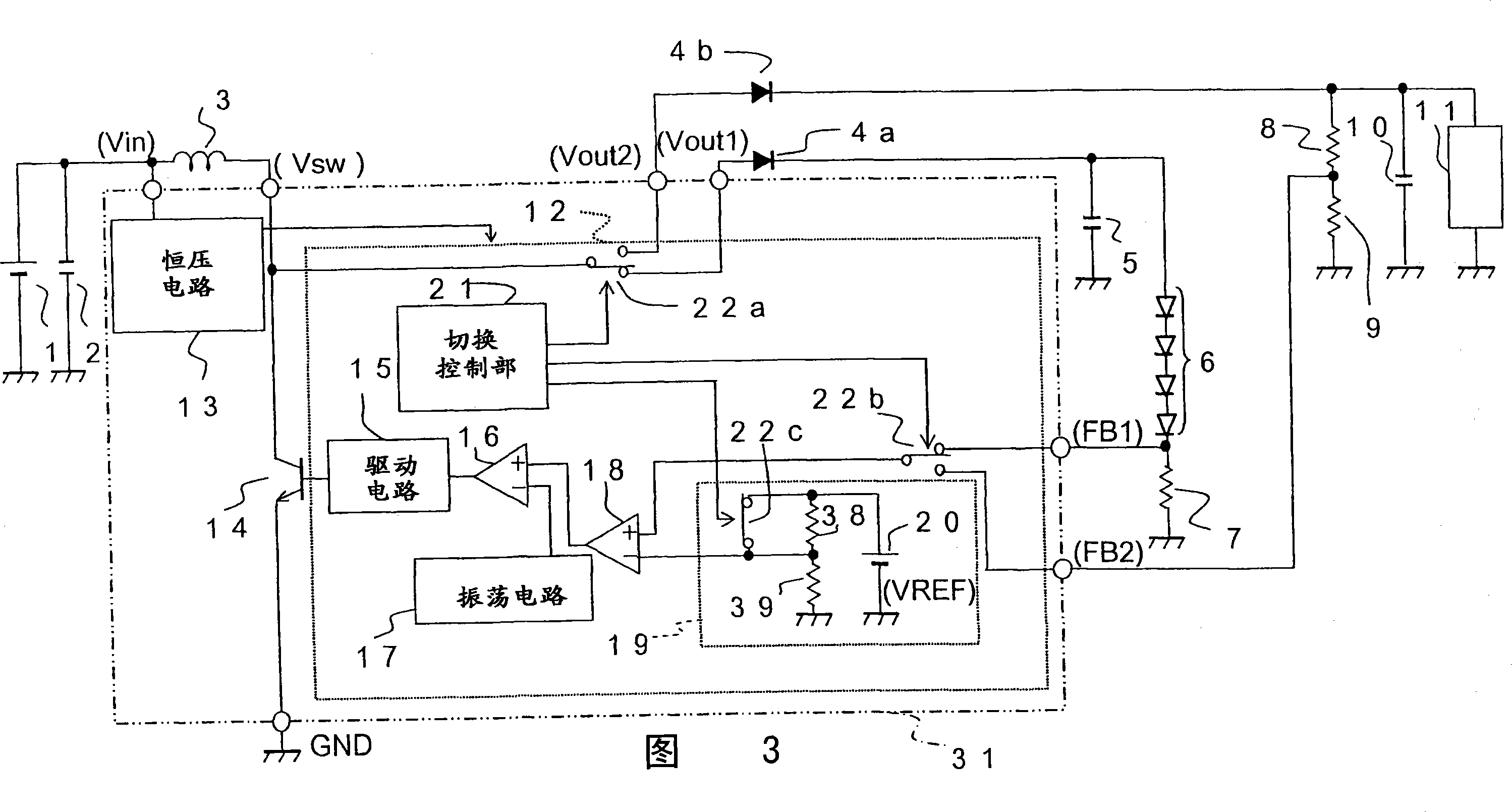
[0084] Embodiment 3: Next, as a third embodiment of the present invention, a power supply circuit will be described again below. The structure here is largely the same as that of Embodiment 1, and the main difference lies in the structure of the reference voltage circuit 19 . Therefore, overlapping descriptions will not be repeated.
[0085] FIG. 3 shows the structure of the power supply circuit of this embodiment. As shown, the reference voltage circuit 19 includes a reference voltage source 20, a resistor 38, a resistor 39, a third switch 22c and other components.
[0086] The reference voltage source 20 generates a predetermined reference voltage VREF, and its negative terminal is grounded. The positive terminal of the reference voltage source 20 is connected to one terminal of the resistor 38 and one terminal of the third switch 22c. The other end of the resistor 38 is grounded via a resistor 39 . The node between the resistors 38 and 39 is connected to the other end o...
PUM
 Abstract
Description
Claims
Application Information


