Transistors and methods of forming them

A technology of transistors and semiconductors, which is applied in the manufacture of transistors, semiconductor devices, semiconductor/solid-state devices, etc., can solve problems such as unfavorable transistor performance, and achieve the effects of easy control, simple process, and improved performance

Active Publication Date: 2016-08-31
SEMICON MFG INT (SHANGHAI) CORP
View PDF5 Cites 0 Cited by
  • Summary
  • Abstract
  • Description
  • Claims
  • Application Information

AI Technical Summary

Problems solved by technology

[0009] However, in the conventionally formed transistor, the work function of the gate electrode 103 is constant across the channel region from the source region 112 to the drain region 113, which is not conducive to improving the performance of the transistor.

Method used


Image

  • Transistors and methods of forming them
  • Transistors and methods of forming them
  • Transistors and methods of forming them

Examples


Embodiment Construction

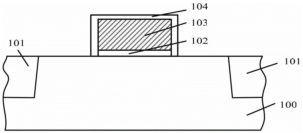
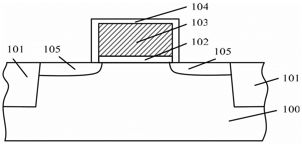
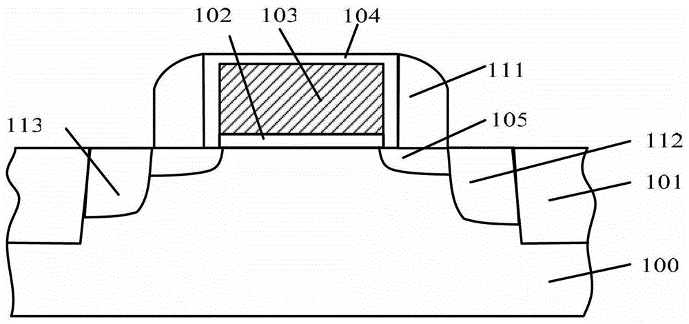
[0034] The work function of the gate electrode of the conventionally formed transistor is constant across the channel region from the source region to the drain region, so that the threshold voltage from the source region to the drain region is constant, and at a fixed gate voltage, the channel The density of carriers in the channel region is the same, which is not conducive to the improvement of transistor performance.

[0035] To this end, the inventor proposes a transistor, the gate electrode of the transistor has a middle region and edge regions located on both sides of the middle region, the gate electrode of the middle region is doped with work function adjusting ions, so that the middle region of the gate electrode The work function of the gate electrode is different from the work function of the edge region of the gate electrode, so that the threshold voltage from the source region to the drain region is different, and at a fixed gate voltage, the total number of carrie...


PUM


Abstract

The invention relates to a transistor and a forming method thereof. The transistor comprises a semiconductor substrate, and a gate structure located on the semiconductor substrate, wherein the gate structure comprises a gate medium layer and a gate electrode located on the surface of the gate medium layer, the gate electrode has a middle region and marginal regions located at both sides of the middle region, and work function adjusting ions are doped in the middle region of the gate electrode, so that the work function of the middle region of the gate electrode is different from work functions of the marginal regions of the gate electrode. Under fixed gate voltage, the density of current carriers in a channel region is improved, and performance of the transistor is improved.

Description

technical field [0001] The invention relates to the field of semiconductor manufacturing, in particular to a transistor and a forming method thereof. Background technique [0002] Metal-oxide-semiconductor (MOS) transistors are the most basic devices in semiconductor manufacturing. They are widely used in various integrated circuits. According to the main carrier and the type of doping during manufacturing, they are divided into NMOS and PMOS transistors. [0003] The prior art provides a method for manufacturing a MOS transistor. Please refer to Figure 1 to Figure 3 The schematic cross-sectional structure diagram of the manufacturing method of the MOS transistor in the prior art is shown. [0004] Please refer to figure 1 , providing a semiconductor substrate 100, forming isolation structures 101 in the semiconductor substrate 100, the semiconductor substrate 100 between the isolation structures 101 is an active region, and forming a doped well (not shown) in the active...

Claims


Application Information

Patent Timeline
Patent Type & Authority Patents(China)
IPC IPC(8): H01L21/336H01L21/328H01L29/78H01L29/423
CPCH01L21/28035H01L29/4916H01L29/4983H01L29/6659H01L29/7833
Inventor 鲍宇平延磊
Owner SEMICON MFG INT (SHANGHAI) CORP
Why Eureka
Try Eureka