

Semiconductor special-purpose equipment wafer grabbing device
A technology of special equipment and grabbing device, which is applied in the manufacture of semiconductor/solid-state devices, manipulators, electrical components, etc., and can solve the problem of high flatness of the surface of the grabbing target, difficulty in processing parts, and difficulty in grabbing wafers, etc. problems, to achieve the effect of easy grasping control, less difficulty in processing, and convenient application
- Summary
- Abstract
- Description
- Claims
- Application Information
AI Technical Summary
Problems solved by technology
Method used
Image

Examples
Embodiment Construction
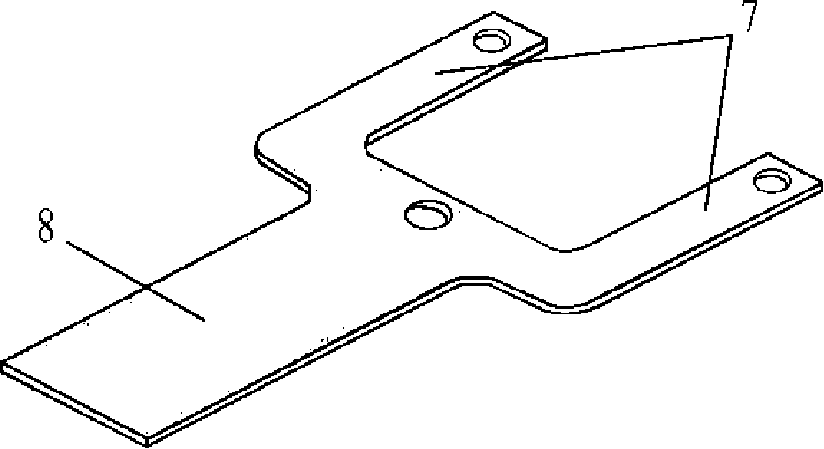
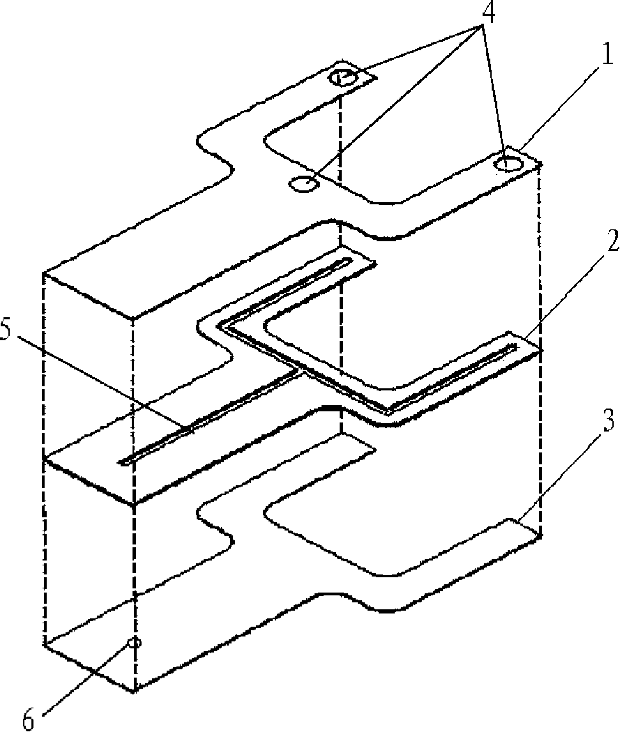
[0015] Examples see figure 1 , 2 As shown, this wafer grabbing device for special semiconductor equipment includes a wafer grabbing plate and a vacuum system connected thereto. In a sheet-like overall structure, a communication groove 5 is opened on the main body core plate 2, and a wafer adsorption hole 4 corresponding to the above-mentioned communication groove 5 is opened on the grasping panel 1, and the sealing cover plate 3 corresponds to the communication groove 5. There is a vacuum port 6 in the position. The wafer adsorption hole 4 on the above-mentioned grasping panel communicates with the communicating groove 5 on the core plate of the main body correspondingly, and the vacuum interface 6 on the cover plate communicates correspondingly with the communicating groove 5 on the core plate of the main body. The communication groove 5 is Y-shaped.
[0016] There are three above-mentioned wafer adsorption holes 4, which are distributed in a triangular shape on the grabbi...
PUM
 Abstract
Description
Claims
Application Information