
Stepping type non-mask digital exposure device based on digital micro-lens array

A technology of digital micromirror array and exposure device, which is applied in photolithographic process exposure device, microlithography exposure equipment, optics, etc., can solve problems such as difficult to meet, low cost, high equipment cost, etc., and achieve strong technical extension and process compatibility, avoiding high cost effects

Inactive Publication Date: 2008-12-10
INST OF OPTICS & ELECTRONICS - CHINESE ACAD OF SCI
View PDF0 Cites 28 Cited by
  • Summary
  • Abstract
  • Description
  • Claims
  • Application Information

AI Technical Summary

Problems solved by technology

Some occasions require lithography technology and equipment with large-area and super-large-area exposure capabilities. Traditional lithography equipment is achieved by increasing the size of the exposure head, but it brings difficulties to uniform illumination and also brings expensive equipment. cost
In addition, in the production and processing of micro-optical elements, for the micro-optical elements with continuous relief surface shape, since its surface shape needs t

Method used


Image

  • Stepping type non-mask digital exposure device based on digital micro-lens array
  • Stepping type non-mask digital exposure device based on digital micro-lens array
  • Stepping type non-mask digital exposure device based on digital micro-lens array

Examples


Embodiment Construction

[0027] The present invention will be described in detail below in conjunction with the accompanying drawings and specific embodiments.

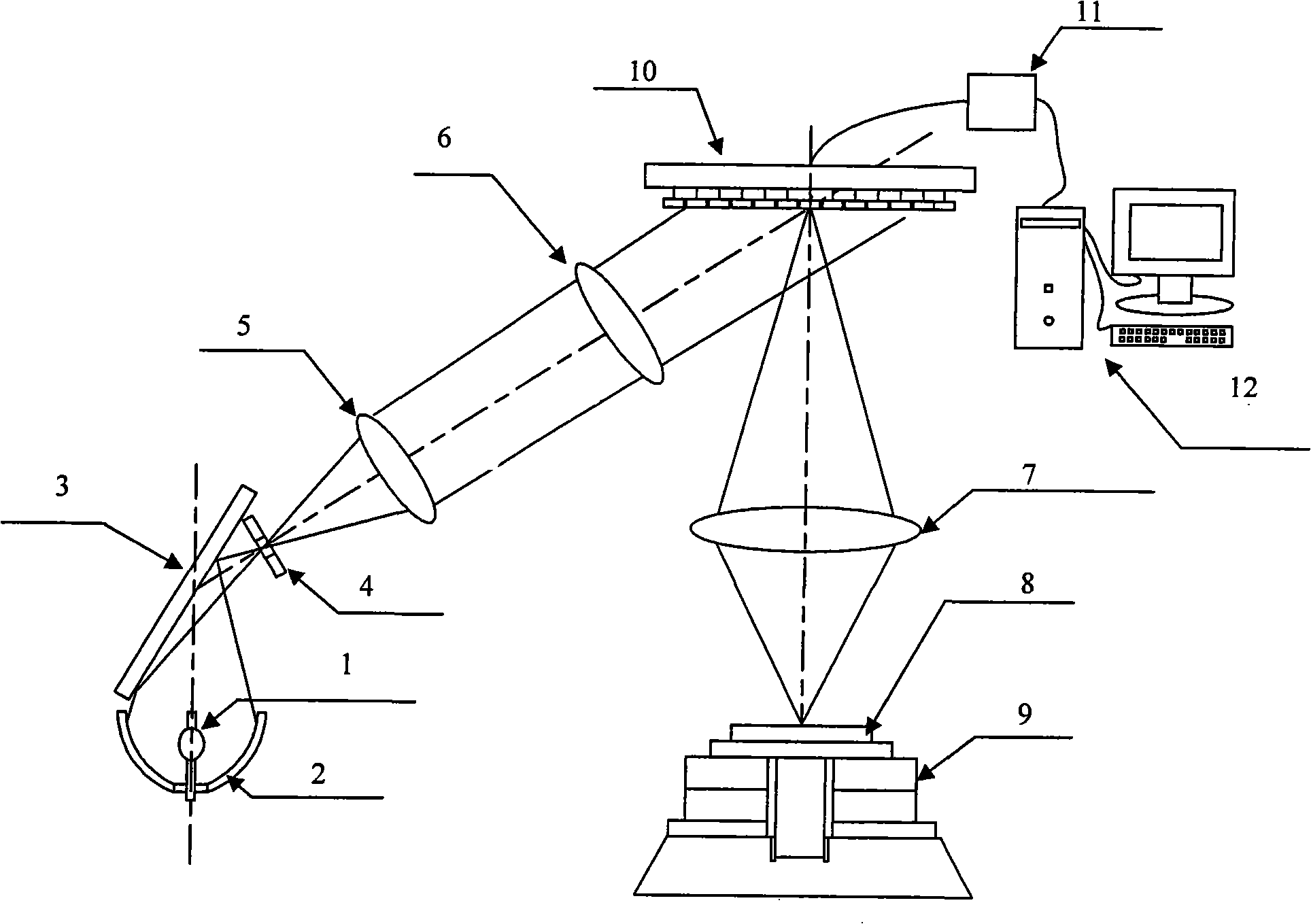
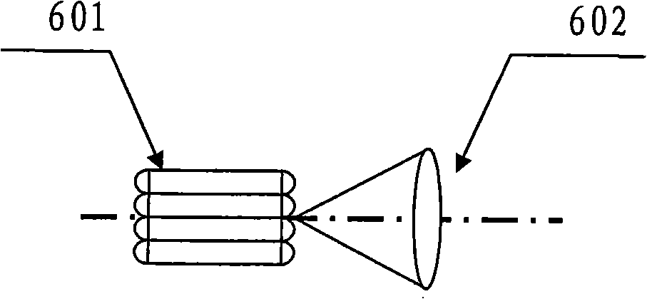
[0028] A step-by-step maskless digital exposure device based on a digital micromirror array in this embodiment is composed of an illumination light source 1, an ellipsoidal mirror 2, a reflector 3, a light block 4, a collimating mirror 5, and an energy integrating homogenizer 6. Projection objective lens 7, lithographic sample 8, X-Y stepping workpiece table 9, digital micromirror array 10, digital micromirror array control card 11, and computer 12; when the lighting source 1 adopts a non-point light source, the light it emits Concentrate the light by the ellipsoidal mirror 2 to ensure that the light energy is fully utilized; the light collected by the ellipsoidal mirror 2 is reflected by the reflector 3 placed at the opening of the ellipsoidal mirror 2 and converges to the light block 4, and the light block 4 will Illumination light source 1...


PUM


Abstract

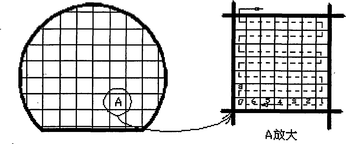
The invention discloses a stepping-type non-mask digital exposure device based on the digital micro-mirror array, which can utilize the method of replacing digital micro-mirror array by a traditional mask plate and combine the characteristics of a projecting exposure system to realize the system digital flexible exposure; patterns and images to be exposed are sent to the digital micro-mirror array by a computer to form a digital mask; then illuminating light treated by homogenization and collimation irradiates the digital micro-mirror array, and the illuminating light is treated by the spatial light modulation by the mask images on the digital micro-mirror array; the patterns and the images on the digital mask plate are copied to a photo-etching sample by a projection objective system; the photo-etching sample is arranged on a high-precision X-Y direction movable work-piece table and steps by the work-piece table; the patterns of all exposure sub-fields are orderly formed on the focal plane by the digital micro-mirror, and are jointed to obtain an exposure image or pattern with larger area. The device has strong technological extensibility and technique compatibility, and is easy to apply to the common engineering practices.

Description

technical field [0001] The invention relates to a maskless digital exposure device, in particular to a step-by-step maskless digital exposure device based on a digital micromirror array. technical background [0002] Original lithography equipment such as: proximity X-ray lithography, extreme ultraviolet projection lithography, electron beam projection lithography, electron beam direct writing, ion projection lithography, immersion optical projection lithography, nanoimprint lithography, etc. The equipment needs to use a mask in lithography, and the traditional mask is easy to be damaged and scratched during use, which affects the exposure quality and production efficiency. Moreover, due to the influence of factors such as expensive mask costs, high exposure device prices, and lack of flexibility, it cannot meet the needs of low-end users such as laboratories for interactive design and flexible processing, thus greatly limiting traditional projection lithography. Scope of a...

Claims


Application Information

Patent Timeline
IPC IPC(8): G03F7/20G02B1/10G02B5/08G02B27/09
Inventor 严伟唐小萍胡松邢薇赵立新杨勇杨文波杨波周绍林陈旺富
Owner INST OF OPTICS & ELECTRONICS - CHINESE ACAD OF SCI
Learn More