Method for packaging small-lot chips

A small-batch, chip-based technology, which is applied in the manufacture of electrical components, circuits, semiconductors/solid-state devices, etc., can solve the problems of reducing the cost of small-batch chip packaging and high packaging costs, and is conducive to popularization and use, reducing packaging design links and costs Reduced effect

Active Publication Date: 2009-04-01
佛山中科芯蔚科技有限公司
View PDF0 Cites 5 Cited by
  • Summary
  • Abstract
  • Description
  • Claims
  • Application Information

AI Technical Summary

Problems solved by technology

[0013] In view of this, the main purpose of the present invention is to provide a method for packaging small-batch chips, that is, a packaging method for smal

Method used


Image

  • Method for packaging small-lot chips
  • Method for packaging small-lot chips
  • Method for packaging small-lot chips

Examples


Embodiment Construction

[0049] In order to make the object, technical solution and advantages of the present invention clearer, the present invention will be described in further detail below in conjunction with specific embodiments and with reference to the accompanying drawings.

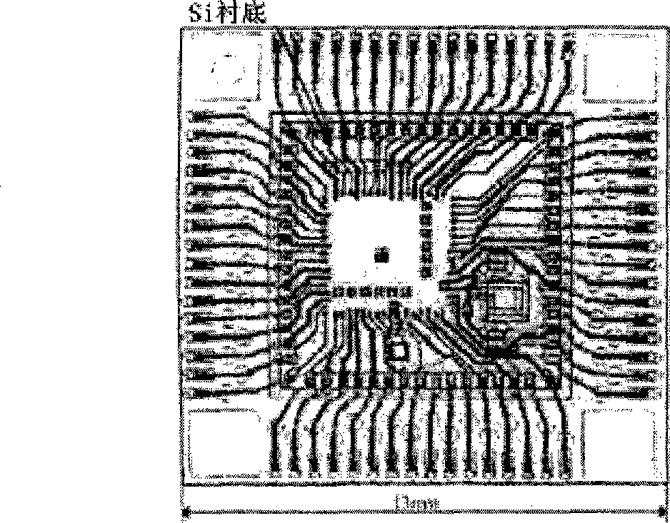
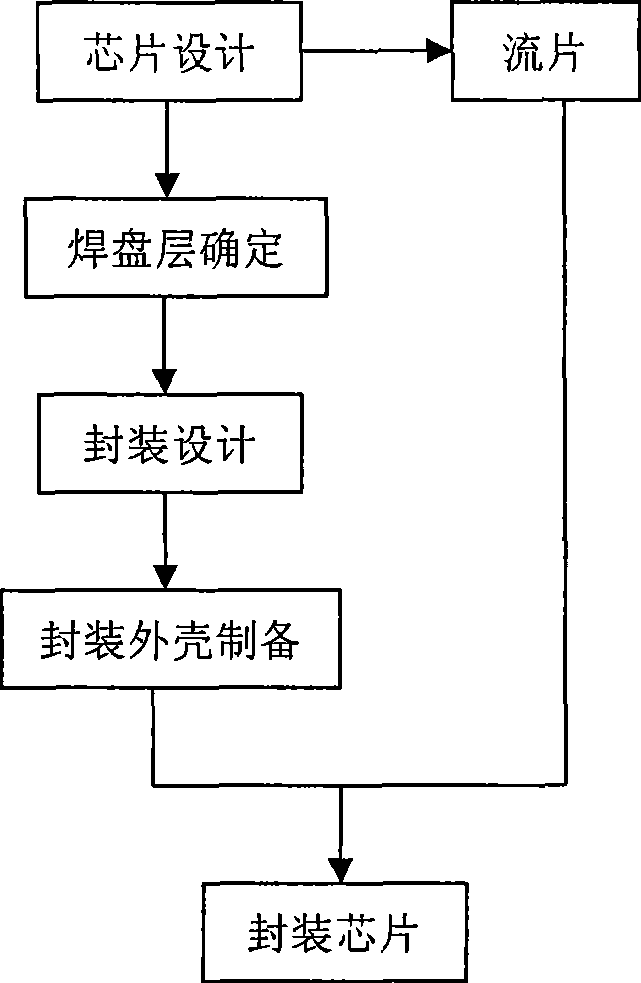
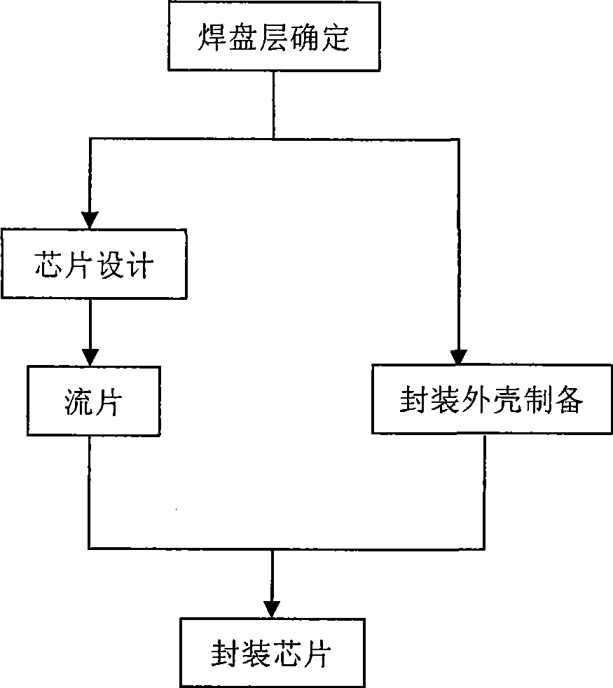
[0050] The semiconductor industry has extremely high requirements on the environment and production accuracy. Using ultra-clean rooms and expensive equipment, chip foundries (foundry factories) and packaging manufacturers have invested hugely, often tens of millions to billions of dollars, designed for large-scale production services. In fact, in addition to commercial large-scale chips, research institutes and many companies need to produce and package small-batch chips for scientific research or new product development. These chips are small in quantity (often only dozens to hundreds of pieces) and have many varieties. Not only do they require separate tape-outs, but they often use different high-end packaging forms. T...


PUM


Abstract

The invention relates to the field of encapsulation technology of micro-electronic chips, and discloses a method for encapsulating small amount of chips; the method comprises: a bonding pad layer is determined according to the pin number and the encapsulation size of the chips; the chip which is in accordance with the requirements of the determined chip bonding pad layer is designed and manufactured, and then a flow piece is manufactured; an encapsulation shell which is in accordance with the requirements of the determined chip bonding pad layer is manufactured; the manufactured flow piece and the encapsulation shell are encapsulated together. By utilizing the invention, the problem that the encapsulation cost of the existing small amount of chips is too high, so that the encapsulation cost of the small amount of chips is reduced.

Description

technical field [0001] The invention relates to the technical field of microelectronic chip packaging, in particular to a method for packaging small-batch chips. Background technique [0002] In today's information age, with the rapid development of the electronic industry, electronic products are required to be multi-functional, high-performance, and miniaturized. With the rapid development of microelectronics technology, the feature size of the integrated circuit (Integrated Circuit, IC) chip is getting smaller and the complexity is increasing, which leads to the pin (Input / output, I / O) of the device and the circuit The number keeps increasing. [0003] Quad Flat Package (QFP) and other four-sided leaded packaging technologies have been widely used in the packaging of semiconductor devices and circuits due to their advantages of low cost and high efficiency. But after entering the 1990s, this kind of packaging technology with leads on four sides can no longer meet the re...

Claims


Application Information

Patent Timeline
IPC IPC(8): H01L21/50
Inventor 陈岚刘杨叶甜春
Owner 佛山中科芯蔚科技有限公司
Why Eureka
Try Eureka