Plasma display device
A display device and plasma technology, applied in identification devices, static indicators, instruments, etc., can solve the problems of display image quality degradation and achieve the effects of improving image quality, high-speed driving, and reducing false discharges
- Summary
- Abstract
- Description
- Claims
- Application Information
AI Technical Summary
Problems solved by technology
Method used
Image

Examples
Embodiment Construction
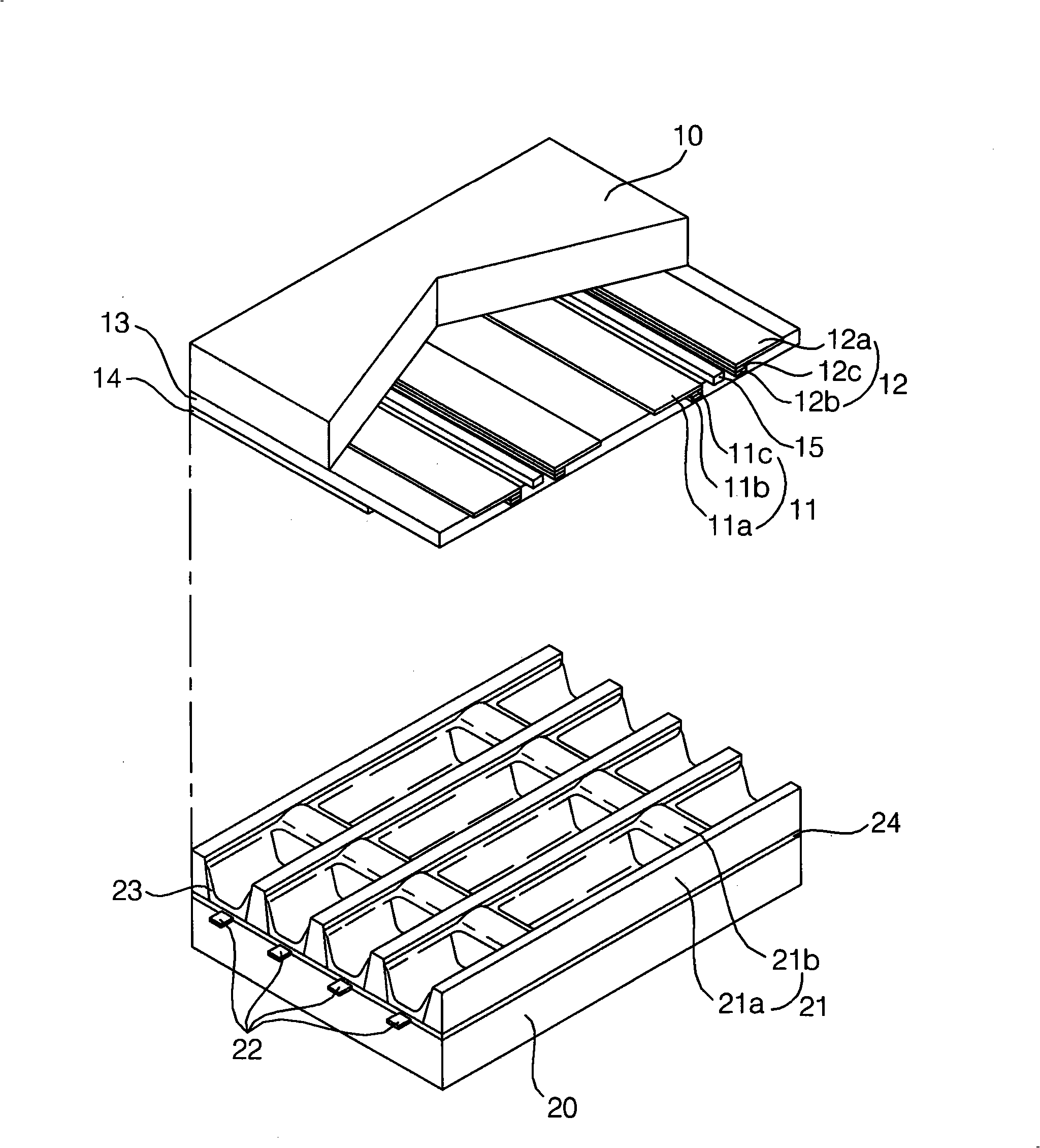
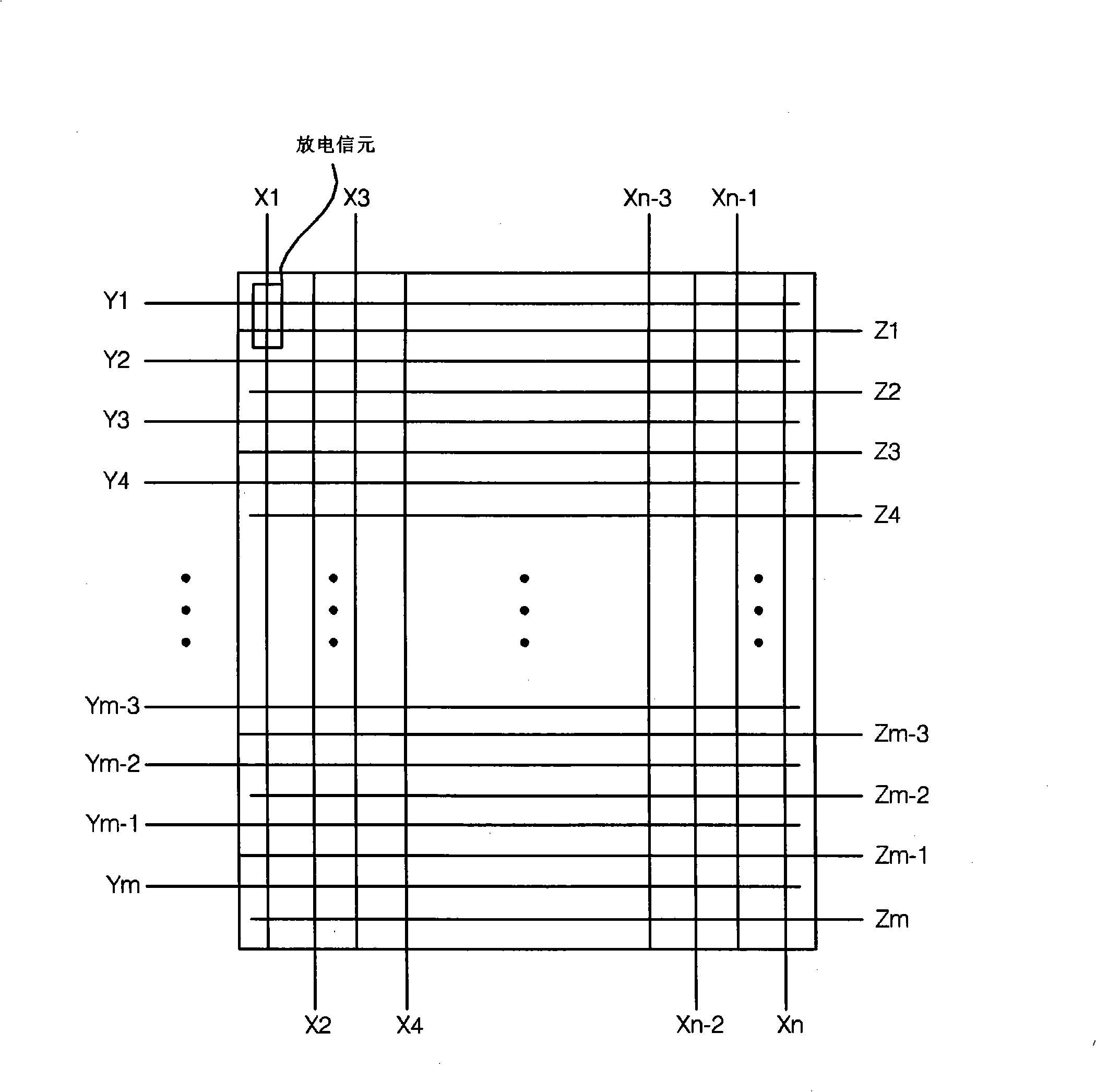
[0017] Hereinafter, the plasma display device in the present invention will be described in detail with reference to preferred embodiments and accompanying drawings. figure 1 It is a schematic diagram of an embodiment of the plasma display panel structure in the present invention.
[0018] like figure 1 As shown, the plasma display panel includes: a pair of sustain electrodes on the upper substrate 10 , that is, a scan electrode 11 and a sustain electrode 12 ; and an address electrode 22 on the lower substrate 20 .
[0019] The above-mentioned sustain electrode pair 11, 12 generally includes transparent electrodes 11a, 12a and bus electrodes 11b, 12b formed by indium tin oxide (Indium-Tin-Oxide; ITO), and the above-mentioned bus electrodes 11b, 12b can be made of silver (Ag ), chromium (Cr) and other metals or chromium / copper / chromium (Cr / Cu / Cr) superposition formed, or chromium / aluminum / chromium (Cr / Al / Cr) superposition formed. The bus electrodes 11b, 12b are located on the...
PUM
 Abstract
Description
Claims
Application Information
 - R&D Engineer
- R&D Manager
- IP Professional
- Industry Leading Data Capabilities
- Powerful AI technology
- Patent DNA Extraction
Browse by: Latest US Patents, China's latest patents, Technical Efficacy Thesaurus, Application Domain, Technology Topic.
© 2024 PatSnap. All rights reserved.Legal|Privacy policy|Modern Slavery Act Transparency Statement|Sitemap